
Specifications


ST72104Gx, ST72215Gx, ST72216Gx, ST72254Gx
133/141
15 DEVICE CONFIGURATION AND ORDERING INFORMATION
Each device is available for production in user pro-
grammable versions (FLASH) as well as in factory
coded versions (ROM). FLASH devices are
shipped to customers with a default content (FFh),
while ROM factory coded parts contain the code
supplied by the customer. This implies that FLASH
devices have to be configured by the customer us
-
ing the Option Bytes while the ROM devices are
factory-configured.
15.1 OPTION BYTES
The two option bytes allow the hardware configu-
ration of the microcontroller to be selected.
The option bytes have no address in the memory
map and can be accessed only in programming
mode (for example using a standard ST7 program
-
ming tool). The default content of the FLASH is
fixed to FFh.
In masked ROM devices, the option bytes are
fixed in hardware by the ROM code (see option
list).
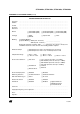
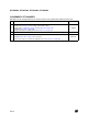
USER OPTION BYTE 0
Bit 7:2 = Reserved, must always be 1.
Bit 1 = EXTIT External Interrupt Configuration.
This option bit allows the external interrupt map-
ping to be configured as shown in Table 23.
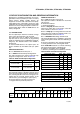
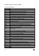
Table 23. External Interrupt Configuration
Bit 0 = FMP Full memory protection.
This option bit enables or disables external access
to the internal program memory (read-out protec
-
tion). Clearing this bit causes the erasing (by over-
writing with the currently latched values) of the
whole memory (not including the option bytes).
0: Program memory not read-out protected
1: Program memory read-out protected
USER OPTION BYTE 1
Bit 7 = CFC Clock filter control on/off
This option bit enables or disables the clock filter
(CF) features.
0: Clock filter enabled
1: Clock filter disabled
Bit 6:4 = OSC[2:0] Oscillator selection
These three option bits can be used to select the
main oscillator as shown in
Table 24.
Bit 3:2 = LVD[1:0] Low voltage detection selection
These option bits enable the LVD block with a se-
lected threshold as shown in Table 25.
Bit 1 = WDG HALT Watchdog and halt mode
This option bit determines if a RESET is generated
when entering HALT mode while the Watchdog is
active.
0: No Reset generation when entering Halt mode
1: Reset generation when entering Halt mode
Bit 0 = WDG SW Hardware or software watchdog
This option bit selects the watchdog type.
0: Hardware (watchdog always enabled)
1: Software (watchdog to be enabled by software)
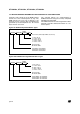
Table 24. Main Oscillator Configuration
Table 25. LVD Threshold Configuration
External IT0 External IT1 EXTIT
Ports PA7-PA0
Ports PB7-PB0
Ports PC5-PC0
1
Ports PA7-PA0
Ports PC5-PC0
Ports PB7-PB0 0
Selected Oscillator OSC2 OSC1 OSC0
External Clock (Stand-by)
1 1 1
~4 MHz Internal RC
1 1 0
1~14 MHz External RC
1 0 X
Low Power Resonator (LP)
0 1 1
Medium Power Resonator (MP)
0 1 0
Medium Speed Resonator (MS)
0 0 1
High Speed Resonator (HS)
0 0 0
Configuration LVD1 LVD0
LVD Off
1 1
Highest Voltage Threshold (∼4.50V)
1 0
Medium Voltage Threshold (∼4.05V)
0 1
Lowest Voltage Threshold (∼3.45V)
0 0
USER OPTION BYTE 0
7
0
USER OPTION BYTE 1
7
0
Reserved EXTIT FMP CFC
OSC
2
OSC
1
OSC
0
LVD1 LVD0
WDG
HALT
WDG
SW
Default
Value
1 1 1 1 1 1 1 0 1 1 1 0 1 1 1 1