
Specifications


ST72104Gx, ST72215Gx, ST72216Gx, ST72254Gx
37/141
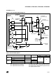
MISCELLANEOUS REGISTERS (Cont’d)
10.3 MISCELLANEOUS REGISTER DESCRIPTION
MISCELLANEOUS REGISTER 1 (MISCR1)
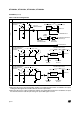
Read / Write
Reset Value: 0000 0000 (00h)
Bit 7:6 = IS1[1:0] ei1 sensitivity
The interrupt sensitivity, defined using the IS1[1:0]
bits, is applied to the ei1 external interrupts. These
two bits can be written only when the I bit of the CC
register is set to 1 (interrupt masked).
ei1: Port B (C optional)
Bit 5 = MCO Main clock out selection
This bit enables the MCO alternate function on the
PC2 I/O port. It is set and cleared by software.
0: MCO alternate function disabled (I/O pin free for
general-purpose I/O)
1: MCO alternate function enabled (f
CPU
on I/O
port)
Bit 4:3 = IS0[1:0] ei0 sensitivity
The interrupt sensitivity, defined using the IS0[1:0]
bits, is applied to the ei0 external interrupts. These
two bits can be written only when the I bit of the CC
register is set to 1 (interrupt masked).
ei0: Port A (C optional)
Bit 2:1 = CP[1:0] CPU clock prescaler
These bits select the CPU clock prescaler which is
applied in the different slow modes. Their action is
conditioned by the setting of the SMS bit. These
two bits are set and cleared by software
Bit 0 = SMS Slow mode select
This bit is set and cleared by software.
0: Normal mode. f
CPU
= f
OSC
/ 2
1: Slow mode. f
CPU
is given by CP1, CP0
See low power consumption mode and MCC
chapters for more details.
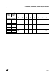
7 0
IS11 IS10 MCO IS01 IS00 CP1 CP0 SMS
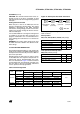
External Interrupt Sensitivity IS11 IS10
Falling edge & low level 0 0
Rising edge only 0 1
Falling edge only 1 0
Rising and falling edge 1 1
External Interrupt Sensitivity IS01 IS00
Falling edge & low level 0 0
Rising edge only 0 1
Falling edge only 1 0
Rising and falling edge 1 1
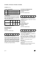
f
CPU
in SLOW mode CP1 CP0
f
OSC
/ 4 0 0
f
OSC
/ 8 1 0
f
OSC
/ 16 0 1
f
OSC
/ 32 1 1