
Specifications


ST72104Gx, ST72215Gx, ST72216Gx, ST72254Gx
8/141
PIN DESCRIPTION (Cont’d)
For external pin connection guidelines, refer to Section 13 "ELECTRICAL CHARACTERISTICS" on page
96.
Legend / Abbreviations for Table 1:
Type: I = input, O = output, S = supply
Input level: A = Dedicated analog input
In/Output level: C = CMOS 0.3V
DD
/0.7V
DD
,
C
T
= CMOS 0.3V
DD
/0.7V
DD
with input trigger
Output level: HS = 20mA high sink (on N-buffer only)
Port and control configuration:
– Input: float = floating, wpu = weak pull-up, int = interrupt
1)
, ana = analog
– Output: OD = open drain
2)
, PP = push-pull
Refer to Section 9 "I/O PORTS" on page 30 for more details on the software configuration of the I/O ports.
The RESET configuration of each pin is shown in bold. This configuration is valid as long as the device is
in reset state.
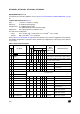
Table 1. Device Pin Description
Pin n°
Pin Name
Type
Level Port / Control
Main
Function
(after reset)
Alternate Function
SDIP32
SO28
Input
Output
Input Output
float
wpu
int
ana
OD
PP
1 1 RESET I/O C
T
X X Top priority non maskable interrupt (active low)
2 2 OSC1
3)
I
External clock input or Resonator oscillator in-
verter input or resistor input for RC oscillator
3 3 OSC2
3)
O
Resonator oscillator inverter output or capaci-
tor input for RC oscillator
4 4 PB7/SS I/O C
T
X ei1 X X Port B7 SPI Slave Select (active low)
5 5 PB6/SCK/ISPCLK I/O C
T
X ei1 X X Port B6 SPI Serial Clock or ISP Clock
6 6 PB5/MISO/ISPDATA I/O C
T
X ei1 X X Port B5
SPI Master In/ Slave Out Data
or ISP Data
7 7 PB4/MOSI I/O C
T
X ei1 X X Port B4 SPI Master Out / Slave In Data
8 NC
Not Connected
9 NC
10 8 PB3/OCMP2_A I/O C
T
X ei1 X X Port B3 Timer A Output Compare 2
11 9 PB2/ICAP2_A I/O C
T
X ei1 X X Port B2 Timer A Input Capture 2
12 10 PB1 /OCMP1_A I/O C
T
X ei1 X X Port B1 Timer A Output Compare 1
13 11 PB0 /ICAP1_A I/O C
T
X ei1 X X Port B0 Timer A Input Capture 1
14 12 PC5/EXTCLK_A/AIN5 I/O C
T
X ei0/ei1 X X Port C5
Timer A Input Clock or ADC
Analog Input 5
15 13 PC4/OCMP2_B/AIN4 I/O C
T
X ei0/ei1 X X Port C4
Timer B Output Compare 2 or
ADC Analog Input 4
16 14 PC3/ ICAP2_B/AIN3 I/O C
T
X ei0/ei1 X X X Port C3
Timer B Input Capture 2 or
ADC Analog Input 3
17 15 PC2/MCO/AIN2 I/O C
T
X ei0/ei1 X X X Port C2
Main clock output (f
CPU
) or
ADC Analog Input 2
6