
Specifications


ST72104Gx, ST72215Gx, ST72216Gx, ST72254Gx
9/141
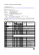
Notes:
1. In the interrupt input column, “eiX” defines the associated external interrupt vector. If the weak pull-up
column (wpu) is merged with the interrupt column (int), then the I/O configuration is pull-up interrupt input,
else the configuration is floating interrupt input.
2. In the open drain output column, “T” defines a true open drain I/O (P-Buffer and protection diode to V
DD
are not implemented). See Section 9 "I/O PORTS" on page 30 and Section 13.8 "I/O PORT PIN CHAR-
ACTERISTICS" on page 118 for more details.
3. OSC1 and OSC2 pins connect a crystal or ceramic resonator, an external RC, or an external source to
the on-chip oscillator see
Section 2 "PIN DESCRIPTION" on page 7 and Section 13.5 "CLOCK AND TIM-
ING CHARACTERISTICS" on page 105 for more details.
18 16 PC1/OCMP1_B/AIN1 I/O C
T
X ei0/ei1 X X X Port C1
Timer B Output Compare 1 or
ADC Analog Input 1
19 17 PC0/ICAP1_B/AIN0 I/O C
T
X ei0/ei1 X X X Port C0
Timer B Input Capture 1 or
ADC Analog Input 0
20 18 PA7 I/O C
T
HS X ei0 X X Port A7
21 19 PA6 /SDAI I/O C
T
HS X ei0 T Port A6 I
2
C Data
22 20 PA5 I/O C
T
HS X ei0 X X Port A5
23 21 PA4 /SCLI I/O C
T
HS X ei0 T Port A4 I
2
C Clock
24 NC
Not Connected
25 NC
26 22 PA3 I/O C
T
HS X ei0 X X Port A3
27 23 PA2 I/O C
T
HS X ei0 X X Port A2
28 24 PA1 I/O C
T
HS X ei0 X X Port A1
29 25 PA0 I/O C
T
HS X ei0 X X Port A0
30 26 ISPSEL I C X
In situ programming selection (Should be tied
low in standard user mode).
31 27 V
SS
S Ground
32 28 V
DD
S Main power supply
Pin n°
Pin Name
Type
Level Port / Control
Main
Function
(after reset)
Alternate Function
SDIP32
SO28
Input
Output
Input Output
float
wpu
int
ana
OD
PP