
Specifications


CC
1100E
SWRS
082
Page
48
of
92
19.5
Wake
O
n Radio (WOR)
The optional Wake on Radio (WOR)
functionality enables
the
CC
1100E
to periodically
wake up from
SLEEP
and listen for incoming
packets without MCU interaction.
When the
SWOR
strobe command is sent on
the SPI interface
, the
CC
1100E
will go to the
SLEEP state when
CSn
is released
.
The RC
oscillator must be enabled before the
SWOR
strobe can be used, as it is the clock source
for the WOR timer.
The on
-
chip timer will
set
the
CC
1100E
into
IDLE state
and then RX state
.
After a programmable time in RX, the chip
will
go
back to
the
SLEEP
state
, unless a packet is
received. See
Figure
23
and
S
ection
19.7
for
details on how the timeout works.
T
o exit WOR mode
, s
et the
CC
1100E
into the
IDLE state
The
CC
1100E
can be set up to signal the MCU
that a packet has been received by using the
GDO pins. If a packet is received, the
MCSM1.RXOFF_MODE
will determine the
behaviour at the end of the received packet.
When the MCU has read the packet, it can put
the chip back into SLEEP with the
SWOR
strobe
from the IDLE state
.
The WOR timer has two events, Event 0 and
Event 1. In the SLEEP state with WOR
activated, reaching Event 0 will turn
on
the
digital regulator and start the crystal oscillator.
Event 1 follows Event 0 after a programmed
timeout.
The time between
two consecutive Event 0 is
programmed with a mantissa value given by
WOREVT1.EVENT0
and
WOREVT0.EVENT0
,
and an exponent value set by
WORCTRL.WOR_RES
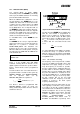
. The equation is:
RES
WOR
XOSC
Event
EVENT
f
t
_
5
0
2
0
750
The Event 1 timeout is programmed with
WORCTRL.EVENT1
.
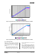
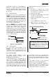
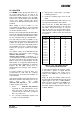
Figure
23
shows the
timing relationship between Event 0 timeout
and Event 1 timeout.
Figure
23
: Event 0 and Event 1 Relationship
The time from the
CC
1100E
en
t
ers SLEEP state
until the next Event0 is programmed to
appear
,
t
SLEEP
in
Figure
23
,
should be larger
than 11.08 ms
when using a 26 MHz crystal
and 10.67 ms when a 27 MHz crystal is used.
If t
SLEEP
is less than 11.08 (10.67) ms
,
there is
a chance that the consecutive Event 0 will
occur
128
750
XOSC
f
seconds
too early. Application Note AN047
[7]
e
xplains
in detail the theory of operation and the
different registers involved when using WOR,
as well as highlighting important aspects when
using WOR mode.
19.5.1
RC Oscillator and T
iming
The frequency of the low
-
power RC oscillator
used for the W
OR functionality varies with
temperature and supply voltage. In order to
keep the frequency as accurate as possible,
the RC oscillator will be calibrated whenever
possible, which is when the XOSC is running
and the chip is not in the SLEEP state. When
the
power and XOSC
are
enabled, the clock
used by the WOR timer is a divided XOSC
clock. When the chip goes to the sleep state,
the RC oscillator will use the last valid
calibration result. The frequency of the RC
oscillator is locked to the main crystal
frequ
ency divided by 750.
In applications where the radio wakes up very
often, typically several times every second, it
is possible to do the RC oscillator calibration
once and then turn off calibration to reduce the
current consumption.
This is done by settin
g
WORCTRL.RC_CAL
=0
and
requires that RC
oscillator calibration values are read from
registers
RCCTRL0_STATUS
and
RCCTRL1_STATUS
and written back
to
RCCTRL0
and
RCCTRL
1
respectively.
If the
Note:
The FIFO
loose
s
its content in the
SLEEP state.