
Specifications


CC
1100E
SWRS
082
Page
89
of
92
30
Package Description (
QFN
20)
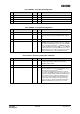
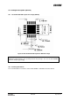
30.1
Recommended PCB
Layout for P
ackage (
QFN
20)
Figure
29
: Recommended PCB
Layout for
QFN
20 P
ackage
30.2
Soldering
I
nformation
The recommendations for lead
-
free reflow in IPC/JEDEC J
-
STD
-
020 should be f
ollowed.
Note:
Figure
29
is an illustration only and not to scale. There are five 10 mil via holes
distributed symmetrically in the ground pad under the package. See also the CC
1100E
EM
reference designs (
[3]
and
[4]
).