
Operating instructions


08/06 9
3.3 Electrical installation
Danger! If the followin
g
instructions are not complied with, there is direct dan
g
e
r
with the possible consequences of death or severe in
j
ury by electrical
current. Further, failure to comply can lead to destruction of the fre-
quency inverter and/or of the expansion module.
• Before electrical installation of the EM-RES-01 expansion module, the frequency
inverter must be de-ener
g
ized. Take appropriate measures to make sure it is not
energized unintentionally.
• Make sure that the frequency inverter is de-energized.
Danger! The mains, direct voltage and motor sockets can have dangerous volta
g
es
even after disconnection of the frequency inverter. Work may only be
done on the device after a waitin
g
period of some minutes until the DC
link capacitors have discharged.
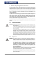
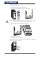
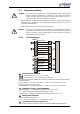
3.3.1 Circuit diagram
6
X410A
X410B
5
6
7
5
EM-RFOUT B+
EM-RFOUT A+
7
3
1
2
4
B
C
D
EM-S1INA
A
D
R
D
GND
CAN-High
CAN-Low
SYS
EM-RFOUT B-
EM-RES SIN+
4
EM-RES REF-
EM-RES REF+
3
1
1
2
2
EM-RES SIN-
EM-RES COS-
EM-RES COS+
EM-RFOUT A-
A
Resolver interface EM-RES
A
1
Field voltage U
REF
eff
= 4 V, I
max
= 60 mA
A
2
Input voltage U
eff
= 2 V, voltage-proof until 30 V
The resolver interface is suitable for connecting commercial resolvers with the follow-
ing specifications:
Input impedance > 95 Ω at 5 kHz, 10 kHz, 20 kHz, no. of pole pairs: up to 24,
30 000 rpm at no. of pole pairs = 1
phase displacement (at field frequency): 7° (5 kHz), 14° (10 kHz), 26° (20 kHz)
B
Repetition frequency output EM-RFOUT
Frequency signal, f
max
= 512 kHz, overload and short-circuit proof,
I
max
= ±60 mA at min. permissible line termination 150 Ω,
TTL (push-pull) according to specification RS-422A / RS-485: U
max
= 5 V
C
Analog input EM-S1INA
Analog signal, resolution 12 Bit,
U
max
= ±10 V (Ri = 100 kΩ), I
max
= ±20 mA (Ri = 250 Ω)
D
Communication interface system bus
CAN actuation of the system bus according to ISO-DIS 11898 (CAN High Speed)