
- TTCAN IP Module User's Manual


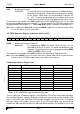
Table Of Contents
- 1. About this Document
- 2. Functional Description
- 3. Programmer’s Model
- 3.1 Hardware Reset Description
- 3.2 CAN Protocol Related Registers
- 3.3 Message Interface Register Sets
- 3.4 Message Handler Registers
- 3.5 Registers for Time Triggered Communication
- 3.5.1 Trigger Memory Access Register (addresses 0x0F & 0x0E)
- 3.5.2 IF1 Data B1 and B2 Registers for Trigger Memory Access
- 3.5.3 TT Operation Mode Register (addresses 0x29 & 0x28)
- 3.5.4 TT Matrix Limits1 Register (addresses 0x2B & 0x2A)
- 3.5.5 TT Matrix Limits2 Register (addresses 0x2D & 0x2C)
- 3.5.6 TT Application Watchdog Limit Register (addresses 0x2F & 0x2E)
- 3.5.7 TT Interrupt Enable Register (addresses 0x31 & 0x30)
- 3.5.8 TT Interrupt Vector Register (addresses 0x33 & 0x32)
- 3.5.9 TT Global Time Register (addresses 0x35 & 0x34)
- 3.5.10 TT Cycle Time Register (addresses 0x37 & 0x36)
- 3.5.11 TT Local Time Register (addresses 0x39 & 0x38)
- 3.5.12 TT Master State Register (addresses 0x3B & 0x3A)
- 3.5.13 TT Cycle Count Register (addresses 0x3D & 0x3C)
- 3.5.14 TT Error Level Register (addresses 0x3F & 0x3E)
- 3.5.15 TUR Numerator Configuration Low Register (addresses 0x57 & 0x56)
- 3.5.16 TUR Denominator Configuration Register (addresses 0x59 & 0x58)
- 3.5.17 TUR Numerator Actual Registers (addresses 0x5B & 0x5A)
- 3.5.18 TT Stop_Watch Register (addresses 0x61 & 0x60)
- 3.5.19 TT Global Time Preset Register (addresses 0x65 & 0x64)
- 3.5.20 TT Clock Control Register (addresses 0x67 & 0x66)
- 3.5.21 TT Sync_Mark Register (addresses 0x69 & 0x68)
- 3.5.22 TT Time Mark Register (addresses 0x6D & 0x6C)
- 3.5.23 TT Gap Control Register (addresses 0x6F & 0x6E)
- 4. CAN Application
- 4.1 Internal CAN Message Handling
- 4.2 Configuration of the Module
- 4.2.1 Configuration of the Bit Timing
- 4.2.1.1 Bit Time and Bit Rate
- 4.2.1.2 Propagation Time Segment
- 4.2.1.3 Phase Buffer Segments and Synchronisation
- 4.2.1.4 Oscillator Tolerance Range
- 4.2.1.5 Configuration of the CAN Protocol Controller
- 4.2.1.6 Calculation of the Bit Timing Parameters
- 4.2.1.7 Example for Bit Timing at high Baudrate
- 4.2.1.8 Example for Bit Timing at low Baudrate
- 4.2.2 Configuration of the Message Memory
- 4.2.1 Configuration of the Bit Timing
- 4.3 CAN Communication
- 5. TTCAN Application
- 6. CPU Interface
- 7. Appendix

User’s Manual
BOSCH
- 11/77 -
Revision 1.6TTCAN
11.11.02
manual_about.fm
set to not valid any time, even when their requested transmission is still pending. The old data
will be discarded when a message is updated before its pending transmission has started.
Depending on the configuration of the Message Object, the transmission of a message may
be requested autonomously by the reception of a remote frame with a matching identifier.
2.3.3 Disabled Automatic Retransmission
According to the CAN Specification (see ISO11898, 6.3.3 Recovery Management), the
TTCAN provides means for automatic retransmission of frames that have lost arbitration or
that have been disturbed by errors during transmission. The frame transmission service will
not be confirmed to the user before the transmission is successfully completed. By default,
this means for automatic retransmission is enabled. It can be disabled to enable the TTCAN to
work within a Time Triggered CAN (TTCAN, see ISO11898-1) environment.
The Disabled Automatic Retransmission mode is enabled by programming bit DAR in the CAN
Control Register to
one
. In this operation mode the programmer has to consider the different
behaviour of bits TxRqst and NewDat in the Control Registers of the Message Buffers:
• When a transmission starts bit TxRqst of the respective Message Buffer is reset, while bit
NewDat remains set.
• When the transmission completed successfully bit NewDat is reset.
When a transmission failed (lost arbitration or error) bit NewDat remains set. To restart the
transmission the CPU has to set TxRqst back to
one
.
Note :
It is not necessary to set DAR if the TTCAN is in time triggered operating mode.
2.3.4 Test Mode
The Test Mode is entered by setting bit Test in the CAN Control Register to
one
. In Test Mode
the bits Tx1, Tx0, LBack, Silent, NoRAM, and WdOff in the Test Register are writable. Bit Rx
monitors the state of pin CAN_RX and therefore is only readable. All Test Register functions
are disabled when bit Test is reset to zero.
Loop Back Mode, No Message RAM Mode, and CAN_TX Control Mode are hardware test
modes, not to be used by application programs.
Silent Mode and the Watchdog Disable Mode are software test modes.
2.3.4.1 Test Register (addresses 0x0B & 0x0A)
StW Monitors the actual value of the STOP_WATCH_TRIGGER pin
EvT Monitors the actual value of the EVENT_TRIGGER pin
Rx Monitors the actual value of the CAN_RX pin
one
The CAN bus is recessive (CAN_RX = ‘1’).
zero
The CAN bus is dominant (CAN_RX = ‘0’).
Tx1-0 Control of CAN_TX pin
00
Reset value, CAN_TX is controlled by the CAN_Core.
01
Sample Point can be monitored at CAN_TX pin.
10
CAN_TX pin drives a dominant (‘0’) value.
11
CAN_TX pin drives a recessive (‘1’) value.
15 14 13 12 11 10 9 8 7 6 5 4 3 2 1 0
StW EvT res res res res res res Rx Tx1 Tx0 LBack Silent NoRAM res WdOff
rrrrrrrrrrwrwrwrwrwrrw