
- TTCAN IP Module User's Manual

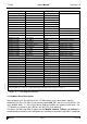

Table Of Contents
- 1. About this Document
- 2. Functional Description
- 3. Programmer’s Model
- 3.1 Hardware Reset Description
- 3.2 CAN Protocol Related Registers
- 3.3 Message Interface Register Sets
- 3.4 Message Handler Registers
- 3.5 Registers for Time Triggered Communication
- 3.5.1 Trigger Memory Access Register (addresses 0x0F & 0x0E)
- 3.5.2 IF1 Data B1 and B2 Registers for Trigger Memory Access
- 3.5.3 TT Operation Mode Register (addresses 0x29 & 0x28)
- 3.5.4 TT Matrix Limits1 Register (addresses 0x2B & 0x2A)
- 3.5.5 TT Matrix Limits2 Register (addresses 0x2D & 0x2C)
- 3.5.6 TT Application Watchdog Limit Register (addresses 0x2F & 0x2E)
- 3.5.7 TT Interrupt Enable Register (addresses 0x31 & 0x30)
- 3.5.8 TT Interrupt Vector Register (addresses 0x33 & 0x32)
- 3.5.9 TT Global Time Register (addresses 0x35 & 0x34)
- 3.5.10 TT Cycle Time Register (addresses 0x37 & 0x36)
- 3.5.11 TT Local Time Register (addresses 0x39 & 0x38)
- 3.5.12 TT Master State Register (addresses 0x3B & 0x3A)
- 3.5.13 TT Cycle Count Register (addresses 0x3D & 0x3C)
- 3.5.14 TT Error Level Register (addresses 0x3F & 0x3E)
- 3.5.15 TUR Numerator Configuration Low Register (addresses 0x57 & 0x56)
- 3.5.16 TUR Denominator Configuration Register (addresses 0x59 & 0x58)
- 3.5.17 TUR Numerator Actual Registers (addresses 0x5B & 0x5A)
- 3.5.18 TT Stop_Watch Register (addresses 0x61 & 0x60)
- 3.5.19 TT Global Time Preset Register (addresses 0x65 & 0x64)
- 3.5.20 TT Clock Control Register (addresses 0x67 & 0x66)
- 3.5.21 TT Sync_Mark Register (addresses 0x69 & 0x68)
- 3.5.22 TT Time Mark Register (addresses 0x6D & 0x6C)
- 3.5.23 TT Gap Control Register (addresses 0x6F & 0x6E)
- 4. CAN Application
- 4.1 Internal CAN Message Handling
- 4.2 Configuration of the Module
- 4.2.1 Configuration of the Bit Timing
- 4.2.1.1 Bit Time and Bit Rate
- 4.2.1.2 Propagation Time Segment
- 4.2.1.3 Phase Buffer Segments and Synchronisation
- 4.2.1.4 Oscillator Tolerance Range
- 4.2.1.5 Configuration of the CAN Protocol Controller
- 4.2.1.6 Calculation of the Bit Timing Parameters
- 4.2.1.7 Example for Bit Timing at high Baudrate
- 4.2.1.8 Example for Bit Timing at low Baudrate
- 4.2.2 Configuration of the Message Memory
- 4.2.1 Configuration of the Bit Timing
- 4.3 CAN Communication
- 5. TTCAN Application
- 6. CPU Interface
- 7. Appendix

User’s Manual
BOSCH
- 18/77 -
Revision 1.6TTCAN
11.11.02
manual_about.fm
3.2.2 Status Register (addresses 0x03 & 0x02)
BOff Bus_Off Status
one
The CAN module is in Bus_Off state.
zero
The CAN module is not Bus_Off.
EWarn Warning Status
one
At least one of the error counters in the EML has reached the error warning
limit of 96.
zero
Both error counters are below the error warning limit of 96.
EPass Error Passive
one
The CAN Core is in the
error passive
state as defined in the CAN Specification.
zero
The CAN Core is
error active
.
RxOk Received a Message Successfully
one
Since this bit was last reset (to zero) by the CPU, a message has been suc-
cessfully received (independent of the result of acceptance filtering).
zero
Since this bit was last reset by the CPU, no message has been successfully
received. This bit is never reset by the CAN Core.
TxOk Transmitted a Message Successfully
one
Since this bit was last reset by the CPU, a message has been successfully
(error free and acknowledged by at least one other node) transmitted.
zero
Since this bit was reset by the CPU, no message has been successfully trans-
mitted. This bit is never reset by the CAN Core.
LEC Last Error Code (Type of the last error to occur on the CAN bus)
0 No Error
1
Stuff Error : More than 5 equal bits in a sequence have occurred in a part of a
received message where this is not allowed.
2
Form Error : A fixed format part of a received frame has the wrong format.
3
AckError : The message this CAN Core transmitted was not acknowledged by
another node.
4
Bit1Error : During the transmission of a message (with the exception of the
arbitration field), the device wanted to send a
recessive
level (bit of logical value
‘1’), but the monitored bus value was
dominant
.
5
Bit0Error : During the transmission of a message (or acknowledge bit, or
active error flag, or overload flag), the device wanted to send a
dominant
level
(data or identifier bit logical value ‘0’), but the monitored bus value was
reces-
sive
. During
Bus_Off
recovery this status is set each time a sequence of 11
recessive
bits has been monitored. This enables the CPU to monitor the pro-
ceeding of the Bus_Off recovery sequence (indicating the bus is not stuck at
dominant
or continuously disturbed).
6
CRCError : The CRC check sum was incorrect in the message received, the
CRC received for an incoming message does not match with the calculated
CRC for the received data.
7 unused : When the LEC shows the value ‘7’, no CAN bus event was detected
since the CPU wrote this value to the LEC.
1514131211109876543210
res res res res res res res res BOff
EWarn
EPass RxOk TxOk LEC
rrrrrrrrrrrrwrw rw