
Information


BNO055
Data sheet
Page 93
BST-BNO055-DS000-14 | Revision 1.4 | June 2016 Bosch Sensortec
© Bosch Sensortec GmbH reserves all rights even in the event of industrial property rights. We reserve all rights of disposal such as copying and passing on
to third parties. BOSCH and the symbol are registered trademarks of Robert Bosch GmbH, Germany.
Note: Specifications within this document are subject to change without notice.
and waits for the 8 bits of data which shall be written to the specified register address. After
the slave acknowledges the data byte, the master generates a stop signal and terminates the
writing protocol.
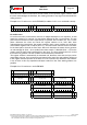
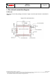
Example of an I²C write access to the BNO055 (i2c address in this case: 0101000b = 0x28):
Figure 6: I²C write
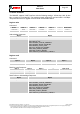
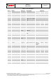
I²C read access:
I²C read access also can be used to read one or multiple data bytes in one sequence. A read
sequence consists of a one-byte I²C write phase followed by the I²C read phase. The two
parts of the transmission must be separated by a repeated start condition (Sr). The I²C write
phase addresses the slave and sends the register address to be read. After slave
acknowledges the transmission, the master generates again a start condition and sends the
slave address together with a read bit (RW = 1). Then the master releases the bus and waits
for the data bytes to be read out from slave. After each data byte the master has to generate
an acknowledge bit (ACK = 0) to enable further data transfer. A NACKM (ACK = 1) from the
master stops the data being transferred from the slave. The slave releases the bus so that
the master can generate a STOP condition and terminate the transmission.
The register address is automatically incremented and, therefore, more than one byte can be
sequentially read out. Once a new data read transmission starts, the start address will be set
to the register address specified in the latest I²C write command. By default the start address
is set at 0x00. In this way repetitive multi-bytes reads from the same starting address are
possible.
Example of an I²C read access to the BNO055:
Figure 7: I²C multiple read
Start RW
ACKS
dummy
ACKS
ACKS
Stop
S 0 1 0 1 0 0 0 0 A x x x x x x x x A x x x x x x x x A P
Slave address
Data
Register address (0x00 .. 0x7F)
Start RW
ACKS
dummy
ACKS
S 0 1 0 1 0 0 0 0 A x 0 0 0 1 0 0 0 A
Start RW
ACKS
ACKM
ACKM
Sr 0 1 0 1 0 0 0 1 A x x x x x x x x A x x x x x x x x A …
ACKS
ACKM
ACKM
… A x x x x x x x x A x x x x x x x x A …
ACKS
ACKM
NACKM
Stop
… A x x x x x x x x A x x x x x x x x NA P
Slave address
Register address (0x08)
Slave address
Read data (0x08)
Read data (0x09)
Read data (0x0A)
Read data (0x0B)
Read data (0x0C)
Read data (0x0D)