
Service manual


Table Of Contents
- COVER
- SELF-DIAGNOSIS FUNCTION
- TABLE OF CONTENTS
- SERVICING NOTES
- GENERAL
- DISASSEMBLY
- TEST MODE
- ELECTRICAL ADJUSTMENTS
- DIAGRAMS
- BLOCK DIAGRAM – SERVO Section –
- BLOCK DIAGRAM – MAIN Section –
- NOTE FOR PRINTED WIRING BOARDS AND SCHEMATIC DIAGRAMS
- Waveforms
- PRINTED WIRING BOARD – BD Board –
- SCHEMATIC DIAGRAM – BD Board (1/2) –
- SCHEMATIC DIAGRAM – BD Board (2/2) –
- PRINTED WIRING BOARD – MAIN Board (Component Side) –
- PRINTED WIRING BOARD – MAIN Board (Conductor Side) –
- SCHEMATIC DIAGRAM – MAIN Board (1/2) –
- SCHEMATIC DIAGRAM – MAIN Board (2/2) –
- PRINTED WIRING BOARD – PANEL Board –
- SCHEMATIC DIAGRAM – PANEL Board –
- IC Block Diagrams
- IC PIN FUNCTION DESCRIPTION
- EXPLODED VIEWS
- ELECTRICAL PARTS LIST
- REVISION HISTORY
6
MDS-NT1
CAUTION
Use of controls or adjustments or performance of procedures
other than those specified herein may result in hazardous ra-
diation exposure.
Notes on chip component replacement
• Never reuse a disconnected chip component.
• Notice that the minus side of a tantalum capacitor may be dam-
aged by heat.
Flexible Circuit Board Repairing
• Keep the temperature of the soldering iron around 270 ˚C dur-
ing repairing.
• Do not touch the soldering iron on the same conductor of the
circuit board (within 3 times).
• Be careful not to apply force on the conductor when soldering
or unsoldering.
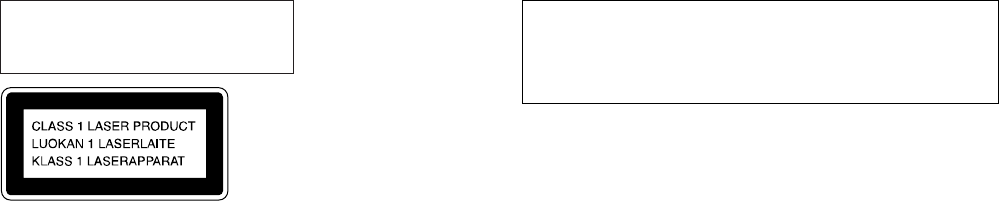
The laser component in this product
is capable of emitting radiation
exceeding the limit for Class 1.
This appliance is classified as a CLASS 1
LASER product. The CLASS 1 LASER
PRODUCT MARKING is located on the
bottom exterior.
SAFETY-RELATED COMPONENT WARNING!!
COMPONENTS IDENTIFIED BY MARK 0 OR DOTTED LINE
WITH MARK 0 ON THE SCHEMATIC DIAGRAMS AND IN
THE PARTS LIST ARE CRITICAL TO SAFE OPERATION.
REPLACE THESE COMPONENTS WITH SONY PARTS WHOSE
PART NUMBERS APPEAR AS SHOWN IN THIS MANUAL
OR IN SUPPLEMENTS PUBLISHED BY SONY.