
Datasheet
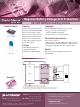
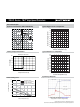
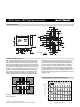
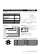
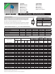
Table Of Contents

Features
■ Superior circuit protection
■ Overcurrent & overvoltage protection
■ Blocks surges up to rated limits
■ High-speed performance
■ Small SMT package
■ RoHS compliant*
■ Agency recognition:
Applications
■ SLIC protection
■ Cable & DSL
■ MDU/MTU modems
■ ONT
■ Voice/DSL line cards
TBU-PL Series - TBU
®
High-Speed Protectors
*RoHS Directive 2002/95/EC Jan. 27, 2003 including annex and RoHS Recast 2011/65/EU June 8, 2011.
Specifi cations are subject to change without notice.
Customers should verify actual device performance in their specifi c applications.
General Information
The TBU-PL Series of Bourns
®
TBU
®
products are low capacitance dual bidirectional high-speed protection
components, constructed using MOSFET semiconductor technology, and designed to protect against faults
caused by short circuits, AC power cross, induction and lightning surges.
In addition to overcurrent protection, an added feature is the voltage monitoring on the two lines. If the voltage
on the line drops below V
ss
then the voltage will trigger the device to switch to the blocking state.
The TBU
®
high-speed protector placed in the system circuit will monitor the current with the MOSFET detec-
tion circuit triggering to provide an effective barrier behind which sensitive electronics will not be exposed to
large voltages or currents during surge events. The TBU
®
device is provided in a surface mount DFN package
and meets industry standard requirements such as RoHS and Pb Free solder refl ow profi les.
Agency Approval
TBU
®
Device
Line 1 SLIC Line 1
Line 2 SLIC Line 2
V
dd
V
ss
Description
UL File Number: E315805
Industry Standards (in Conjunction with OVP Device)
Absolute Maximum Ratings (@ T
A
= 25 °C Unless Otherwise Noted)
Symbol Parameter Part Number Value Unit
V
imp
Peak impulse voltage withstand with duration less than 10 ms
TBU-PL050-xxx-WH
TBU-PL060-xxx-WH
TBU-PL075-xxx-WH
TBU-PL085-xxx-WH
500
600
750
850
V
V
rms
Continuous A.C. RMS voltage
TBU-PL050-xxx-WH
TBU-PL060-xxx-WH
TBU-PL075-xxx-WH
TBU-PL085-xxx-WH
300
350
400
425
V
T
op
Operating temperature range -55 to +125 °C
T
stg
Storage temperature range -65 to +150 °C
T
jmax
Maximum Junction Temperature +125 °C
ESD HBM ESD Protection per IEC 61000-4-2 on line pads ±2 kV
Electrical Characteristics (@ T
A
= 25 °C Unless Otherwise Noted)
Symbol Parameter Part Number Min. Typ. Max. Unit
I
trigger
Current required for the device to go from
operating state to protected state
TBU-PLxxx-100-WH
TBU-PLxxx-200-WH
100
200
150
300
200
400
mA
R
device
Series resistance of the TBU
®
device 40 50 55
Ω
R
match
Package resistance matching of the TBU
®
device #1 - TBU
®
device #2 ±0.5 ±1.0
Ω
t
block
Time taken for the device to go into current limiting 1 µs
I
Q
Current through the triggered TBU
®
device with 50 Vdc circuit voltage 0.25 0.70 1.50 mA
I
ss
Operating current with V
ss
= -50 V 100 µA
V
reset
Voltage below which the triggered TBU
®
device will transition to normal operating state
TBU-PLxxx-100-WH
Forward Mode 12 15 22
V
Reverse Mode 10 13 20
TBU-PLxxx-200-WH
Forward Mode 15 20 25
Reverse Mode 12 17 22
V
to
Voltage threshold offset with 60 Hz applied voltage, with V
ss
-50 V (V
ss
- V
lineSLIC
) -1.0 0.2 V
V
ss
Operating voltage range relative to V
dd
-180 -20 V
R
th(j-l)
One side junction to package pads - FR4 using minimum recommended pad layout 110
°C/W
R
th(j-l)
Both sides junction to package pads - FR4 using minimum recommended pad layout 65
°C/W
R
th(j-l)
One side junction to package pads - FR4 using heat sink on board (6 cm
2
) (0.5 in.
2
) 70
°C/W
R
th(j-l)
Both sides junction to package pads - FR4 using heat sink on board (6 cm
2
) (0.5 in.
2
) 40
°C/W
*RoHS COMPLIANT
L501
C954
Solutions available for GR-1089-CORE, ITU-T and a combination of both.