
Datasheet


6
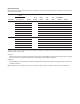
Absolute Maximum Ratings
Parameter Symbol Min. Max. Units Note
Storage Temperature T
S
-55 125 °C
Operating Temperature T
A
-30 100 °C
Average Forward Current I
F(AVG)
- ±50 mA
Input Power Dissipation P
I
- 70 mW
Collector Current I
C
- 50 mA
Collector-Emitter Voltage V
CEO
- 70 V
Emitter-Collector Voltage V
ECO
- 6 V
Isolation Voltage (AC for 1min, R.H. 40~60%) V
ISO
- 5000 V
RMS
Collector Power Dissipation P
C
- 150 mW
Total Power Dissipation P
TOT
- 200 mW
Lead Solder Temperature 260°C for 10 sec., 1.6 mm below seating plane
Electrical Specications (DC)
Over recommended operating conditions unless otherwise specied.
Parameter Symbol Min. Typ. Max. Units Test Conditions Note
Forward Voltage V
F
- 1.2 1.4 V I
F
= ±20mA
Terminal Capacitance C
t
50 250 pF V = 0, f = 1KHz
Collector Dark Current I
CEO
- 100 nA V
CE
= 20V, I
F
= 0 mA
Collector-Emitter Breakdown Voltage B
VCEO
70 - - V I
C
= 0.1 mA, I
F
= 0 mA
Emitter-Collector Breakdown Voltage B
VECO
6 - - V I
E
= 10 mA, I
F
= 0 mA
Collector Current I
C
0.2 - 3 mA I
F
= ±1mA, V
CE
= 5V CTR=(I
C
/I
F
)* 100%
Current Transfer Ratio CTR 20 - 300 %
Collector-Emitter Saturation Voltage V
CE(sat)
- 0.1 0.2 V I
F
= ± 20 mA, I
C
= 1mA
Isolation Resistance R
ISO
5x10
10
1x10
11
-
W
DC500V, R.H. 40~60%
Floating Capacitance C
F
- 0.6 1 pF V = 0, f = 1MHz
Cut-o Frequency (-3dB) F
C
15 80 - KHz V
CE
= 5V, I
C
= 2 mA, R
L
= 100W See g 13
Response Time (Rise) t
r
- 4 18 ms V
CE
= 2V, I
C
= 2 mA, R
L
= 100W See g 12
Response Time (Fall) t
f
- 3 18 ms
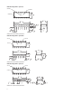
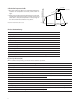
Solder Reow Temperature Prole
1. One-time soldering reow is recommended within the
condition of temperature and time prole shown at
right.
2. When using another soldering method such as infrared
ray lamp, the temperature may rise partially in the mold
of the device. Keep the temperature on the package of
the device within the condition of (1) above.
Note: Non-halide ux should be used
30 seconds
60 ~ 150 sec 90 sec 60 sec
60 sec
25°C
150°C
200°C
250°C
260 °C (Peak Temperature)
217°C
Time (sec)
Temperature
(
°
C)