
Datasheet
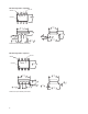

tr
tf
td
ts
L
CEO
CE
V =2V
Ic=2mA
Ta=25 C
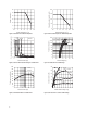
Load resistance R (k
Ω
)
Ambient temperature Ta ( C)
Response time (
µ
s)
Collector dark current I (A)
-10
o
o
10
-25
0.2
0.050 25 50 75 100
10
10
10
10
10
10
-9
-8
-7
-6
-5
-11
0.1 0.2 0.5 1 2 5 10
0.5
1
2
5
10
20
50
100
200
500
CE
V =20V
R =10k
Ω
L
1k
Ω
100
Ω
V =2V
Ic=2mA
Ta=25 C
CE
Frequency f (kHz)
Voltage gain Av (dB
)
o
0.5
20
10
0
2 10 100 5001 5 20 50
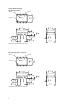
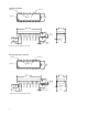
Vcc
R
D
Input
R
D
R
L
L
Vcc
R
Output
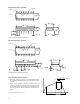
td
Output
Output
Input
tr tf
ts
90%
10%
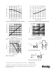
Figure 9. Collector Dark Current vs. Ambient Temperature
Figure 10. Response Time vs. Load Resistance
Figure 12. Test Circuit for Response Time
Figure 11. Frequency Response
Figure 13. Test Circuit for Frequency Response
0
-30
CE
I =5mA
V =5V
CE
F
F
Ic=1mA
I =20mA
Ambient temperature Ta ( C) Ambient temperature Ta ( C)
Relative current transfer ratio (%)
Collector-emitter saturation voltage V (sat) (V)
o
o
0 25 50 75 100
50
100
150
-25
0
0 25 50 75 100
0.02
0.04
0.06
0.08
0.10
0.12
0.14
0.16
Figure 7. Relative Current Transfer Ratio vs. Ambient Temperature
Figure 8. Collector-emitter Saturation Voltage vs. Ambient Temperature
For product information and a complete list of distributors, please go to our web site: www.avagotech.com
Avago, Avago Technologies, and the A logo are trademarks of Avago Technologies in the United States and other countries.
Data subject to change. Copyright © 2005-2008 Avago Technologies. All rights reserved. Obsoletes AV01-0612EN
AV02-1429EN - July 16, 2008