
Datasheet


14
Serial/Simultaneous Data Output D
0
Bit D
0
of control word 1 is used to switch the mode of
D
OUT
between serial and simultaneous data entry during
Control Register writes. The default mode (logic low) is
the serial D
OUT
mode. In serial mode, D
OUT
is connected
to the last bit (D
7
) of the Control Shift Register.
Storing logic high to bit D
0
changes D
OUT
to
simultaneous mode, which aects the Control Register
only. In simultaneous mode, D
OUT
is logically connected
to D
IN
. This arrange ment allows multiple ICs to have their
Control Registers written to simultaneously. For example,
for n ICs in the serial mode, n * 8 clock pulses are needed
to load the same data in all Control Registers. In the
simultaneous mode, n ICs only need 8 clock pulses to
load the same data in all Control Registers. The propaga-
tion delay from the rst IC to the last is n * t
DOUTP
.
External Oscillator Prescaler Bit D
1
Bit D
1
of Control Word 1 is used to scale the frequency of
an external Display Oscillator. When this bit is logic low,
the external Display Oscillator directly sets the internal
display clock rate. When this bit is logic high, the external
oscillator is divided by 8. This scaled frequency then sets
the internal display clock rate. It takes 512 cycles of the
display clock (or 8 x 512 = 4096 cycles of an external clock
with the divide by 8 prescaler) to completely refresh the
display once. Using the prescaler bit allows the designer
to use a higher external oscillator frequency without
extra circuitry.
This bit has no aect on the internal Display Oscillator
Frequency.
Bits D
2
-D
6
These bits must always be pro-grammed to logic low.
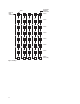
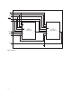
Cascaded ICs
Figure 8 shows how two ICs are connected within an
HCMS-39XX display. The rst IC controls the four left-
most characters and the second IC controls the four
right-most characters. The Dot Registers are connected
in series to form a 320-bit dot shift register. The location
of pixel 0 has not changed. However, Dot Shift Register
bit 0 of IC2 becomes bit 160 of the 320-bit dot shift
register.
The Control Registers of the two ICs are independent
of each other. This means that to adjust the display
brightness the same control word must be entered
into both ICs, unless the Control Registers are set to
simultaneous mode.
Longer character string systems can be built by cascading
multiple displays together. This is accom plished by
creating a ve-line bus. This bus consists of CE, RS, BL,
Reset, and CLK. The display pins are connected to the
corresponding bus line. Thus, all CE pins are connected
to the CE bus line. Similarly, bus lines for RS, BL, Reset,
and CLK are created. Then D
IN
is connected to the right-
most display. D
OUT
from this display is connected to the
next display. The left-most display receives its D
IN
from
the D
OUT
of the display to its right. D
OUT
from the left-
most display is not used.
Each display may be set to use its internal oscillator, or
the displays may be synchronized by setting up one
display as the master and the others as slaves. The slaves
are set to receive their oscillator input from the master’s
oscillator output.