
Datasheet


10
Absolute Maximum Ratings
Parameter Symbol Min. Max. Units Note
Storage Temperature T
S
-55 125 °C
Operating Temperature T
A
-40 85 °C
Average Forward Input Current I
F(AVG)
10 mA 1
Peak Transient Input Current
(≤ 1 µs Pulse Width, 300 pps) I
F(TRAN)
1.0 A 1
(≤ 200 µs Pulse Width, HCNW22XX 40 mA
< 1% Duty Cycle)
Reverse Input Voltage V
R
5 V 1
HCNW22XX 3
Average Output Current I
O
25 mA 1
Supply Voltage V
CC
0 20 V
Output Voltage V
O
-0.5 20 V 1
Total Package Power Dissipation P
T
210 mW 2
HCPL-223X 294
Output Power Dissipation P
O
See Figure 7 1
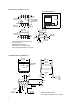
Lead Solder Temperature (Through Hole Parts Only) 260°C for 10 sec.,
1.6 mm below seating plane
HCNW22XX 260°C for 10 sec., up to seating plane
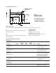
Solder Reow Temperature Prole See Package Outline Drawings section
(Surface Mount Parts Only)
Recommended Operating Conditions
Parameter Symbol Min. Max. Units
Power Supply Voltage V
CC
4.5 20 V
Forward Input Current (ON) I
F(ON)
1.6* 5 mA
HCPL-223X 1.8†
Forward Input Voltage (OFF) V
F(OFF)
- 0.8 V
Operating Temperature T
A
-40 85 °C
Junction Temperature T
J
-40 125 °C
Fan Out N 4 TTL Loads
*The initial switching threshold is 1.6 mA or less. It is recommended that 2.2 mA be used to permit at least a 20% LED degradation guardband.
†The initial switching threshold is 1.8 mA or less. It is recommended that 2.5 mA be used to permit at least a 20% LED degradation guardband.