
Datasheet


11
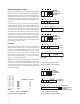
Table 2. Current Requirements at Dierent Brightness Levels for All Colors Except AlGaAs
% V
DD
= 5.0 V
Symbol D
2
D
1
D
0
Brightness 25°C Typ. Units
I
DD
(V) 0 0 0 100 200 mA
0 0 1 80 160 mA
0 1 0 53 106 mA
0 1 1 40 80 mA
1 0 0 27 54 mA
1 0 1 20 40 mA
1 1 0 13 26 mA
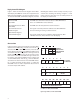
Control Word Register
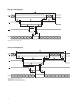
Figure 6 shows how to access the Control Word Register.
This is an eight bit register which performs ve functions.
They are Brightness control, Flash RAM control, Blinking,
Self Test and Clear. Each function is independent of the
others. However, all bits are updated during each Control
Word write cycle.
Brightness (Bits 0-2)
Bits 0-2 of the Control Word adjust the brightness of the
display. Bits 0-2 are interpreted as a three bit binary code
with code (000) corresponding to maximum brightness
and code (111) corresponding to a blanked display. In
addition to varying the display brightness, bits 0-2 also
vary the average value of I
DD
. I
DD
can be calculated at
any brightness level by multiplying the percent bright-
ness level by the value of I
DD
at the 100% brightness level.
These values of I
DD
are shown in Table 2.
Flash Function (Bit 3)
Bit 3 determines whether the ashing character attribute
is on or o. When bit 3 is a “1,” the output of the Flash RAM
is checked. If the content of a location in the Flash RAM is
a “1,” the associated digit will ash at approximately 2 Hz.
For an external clock, the blink rate can be calculated by
dividing the clock frequency by 28,672. If the ash enable
bit of the Control Word is a “0,” the content of the Flash
RAM is ignored. To use this function with multiple display
systems see the Reset section.
Blink Function (Bit 4)
Bit 4 of the Control Word is used to synchronize blinking of
all eight digits of the display. When this bit is a “1” all eight
digits of the display will blink at approximately 2 Hz. The
actual rate is dependent on the clock frequency. For an
external clock, the blink rate can be calculated by dividing
the clock frequency by 28,672. This function will override
the Flash function when it is active. To use this function
with multiple display systems see the Reset section.
Figure 6. Logic levels to access the control word register.
CE
FL A
4
A
3
A
2
A
1
A
0
RST WR RD
01
0 0
0 1
1
1 0 X X X1
0
1 1
UNDEFINED
CONTROL SIGNALS
CONTROL WORD ADDRESS
CONTROL WORD DATA FORMAT
0 = LOGIC 0; 1 = LOGIC 1; X = DO NOT CARE
0 DISABLE FLASH
1 ENABLE FLASH
BRIGHTNESS
CONTROL
LEVELS
0 DISABLE BLINKING
1 ENABLE BLINKING
0 NORMAL OPERATION
1 CLEAR FLASH AND CHARACTER RAMS
0 X NORMAL OPERATION; X IS IGNORED
1 X START SELF TEST; RESULT GIVEN IN X
X = 0 FAILED X = 1 PASSED
WRITE TO DISPLAY
READ FROM DISPLAY
UNDEFINED
D
7
D
6
D
5
D
4
D
3
D
2
D
1
D
0
C
S S BL F B
0 0 0 100%
0 0 1 80%
0 1 0 53%
0 1 1 40%
1 0 0 27%
1 0 1 20%
1 1 0 13%
1 1 1 0%
B B