
Datasheet


2
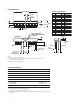
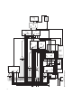
Package Dimensions
Absolute Maximum Ratings
Supply Voltage, V
DD
to Ground
[1]
-0.3 V to 7.0 V
Operating Voltage, V
DD
to Ground
[2]
5.5 V
Input Voltage, Any Pin to Ground -0.3 V to V
DD
+0.3 V
Free Air Operating Temperature Range, T
A
[3 ]
-40°C to + 85°C
Relative Humidity (Noncondensing) 85%
Storage Temperature Range, T
S
-55°C to 100°C
Soldering Temperature [1.59 mm (0.063 in.) Below Body]
Solder Dipping 260°C for 5 secs
Wave Soldering 250°C for 3 secs
ESD Protection @ 1.5 kΩ, 100 pF 4 kV (each pin)
Notes:
1. Maximum voltage is with no LEDs illuminated.
2. 20 dots ON in all locations at full brightness.
3. See Thermal Considerations section for information about operation in high temperature
ambients.
Notes:
1. Dimensions are in mm (inches).
2. Unless otherwise specied, tolerance on dimensions is ±0.25 mm (0.010 inch).
3. For yellow and green displays only.
4. Marking is on side opposite pin 1.
PIN # 15
SYM.
TYP.
DATE CODE (YEAR, WEEK)
LUMINOUS INTENSITY CATEGORY
COLOR BIN (3)
3.81
(0.150)
PIN # 16
1.52
(0.060)
5.31
(0.209)
2.29
(0.090)
4.57
(0.180)
[4]
4.01
(0.158)
SYM.
5.08
(0.200)
10.16
(0.400)
TYP.
0.46 0.13
(0.018 0.005)
TYP.
PIN #1
PART NUMBER
2.54 0.13
(0.100 0.005)
(TOL. NON ACCUM.)
7.62
(0.300)
REF.
0.25
(0.010)
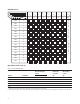
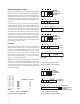
PIN # FUNCTION PIN # FUNCTION
1
2
3
4
5
6
7
8
9
10
11
12
13
14
15
RST
FL
A0
A1
A2
A3
NO PIN
NO PIN
NO PIN
A4
CLS
CLK
WR
CE
V
DD
16
17
18
19
20
21
22
23
24
25
26
27
28
29
30
GND (SUPPLY)
THERMAL TEST
GND (LOGIC)
RD
D0
D1
NO PIN
NO PIN
NO PIN
D2
D3
D4
D5
D6
D7
PIN FUNCTION ASSIGNMENT TABLE
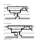
3 4 5 6 7
TYP.
SYM.
11.43
(0.450)
MAX.
TYP.
2.54
(0.100)
SYM.
2.68
(0.105)
42.93 (1.690) MAX.
TYP.
5.36
(0.211)
PIN #15
PIN #1 IDENTIFIER
HDSP-253x X Z
YYWW
210