
Datasheet


5
Symbol Description 25°C Typical Minimum
[1]
Units
F
OSC
Oscillator Frequency 57 28 kHz
F
RF
[5]
Display Refresh Rate 256 128 Hz
F
FL
[6]
Character Flash Rate 2 1 Hz
t
ST
[7]
Self Test Cycle Time 4.6 9.2 sec
Notes:
5. F
RF
= F
OSC
/224.
6. F
FL
= F
OSC
/28,672.
7. t
ST
= 262,144/F
OSC
.
AC Timing Characteristics over Temperature Range
V
DD
= 4.5 to 5.5 V unless otherwise specied.
Reference
Number Symbol Description Min.
[1]
Units
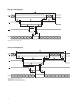
1 t
ACC
Display Access Time
Write 210
Read 230 ns
2 t
ACS
Address Setup Time to Chip Enable 10 ns
3 t
CE
Chip Enable Active Time
[2, 3]
Write 140
Read 160 ns
4 t
ACH
Address Hold Time to Chip Enable 20 ns
5 t
CER
Chip Enable Recovery Time 60 ns
6 t
CES
Chip Enable Active Prior to Rising Edge of
[2, 3]
Write 140
Read 160 ns
7 t
CEH
Chip Enable Hold Time to Rising Edge of Read/Write Signal
[2,3]
0 ns
8 t
W
Write Active Time 100 ns
9 t
WD
Data Valid Prior to Rising Edge of Write Signal 50 ns
10 t
DH
Data Write Hold Time 20 ns
11 t
R
Chip Enable Active Prior to Valid Data 160 ns
12 t
RD
Read Active Prior to Valid Data 75 ns
13 t
DF
Read Data Float Delay 10 ns
t
RC
Reset Active Time
[4]
300 ns
Notes:
1. Worst case values occur at an IC junction temperature of 125°C.
2. For designers who do not need to read from the display, the Read line can be tied to V
DD
and the Write and Chip Enable lines can be tied
together.
3. Changing the logic levels of the Address lines when CE = “0” may cause erroneous data to be entered into the Character RAM, regardless of the
logic levels of the WR and RD lines.
4. The display must not be accessed until after 3 clock pulses (110 µs min. using the internal refresh clock) after the rising edge of the reset line.