
Datasheet


7
Electrical Description
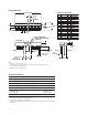
Pin Function Description
RESET (RST, pin 1) Reset initializes the display.
FLASH (FL, pin 2) FL low indicates an access to the Flash RAM and is unaected by the state of address
lines A
3
-A
4
.
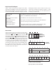
ADDRESS INPUTS Each location in memory has a distinct address. Address inputs (A
0
-A
2
) select a specic
(A
0
-A
4
, pins 3-6, 10) location in the Character RAM, the Flash RAM or a particular row in the UDC (User-
Dened Character) RAM. A
3
-A
4
are used to select which section of memory is accessed.
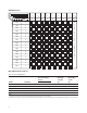
Table 1 shows the logic levels needed to access each section of memory.
Table 1. Logic Levels to Access Memory
FL A
4
A
3
Section of Memory A
2
A
1
A
0
0 X X Flash RAM Character Address
1 0 0 UDC Address Register Don’t Care
1 0 1 UDC RAM Row Address
1 1 0 Control Word Register Don’t Care
1 1 1 Character RAM Character Address
CLOCK SELECT (CLS, pin 11) This input is used to select either an internal (CLS = 1) or external (CLS = 0) clock source.
CLOCK INPUT/OUTPUT Outputs the master clock (CLS = 1) or inputs a clock (CLS = 0) for slave displays.
(CLK, pin 12)
WRITE (WR, pin 13) Data is written into the display when the WR input is low and the CE input is low.
CHIP ENABLE (CE, pin 14) This input must be at a logic low to read or write data to the display and must go high
between each read and write cycle.
READ (RD, pin 19) Data is read from the display when the RD input is low and the CE input is low.
DATA Bus The Data bus is used to read from or write to the display.
(D
0
-D
7
, pins 20, 21, 25-30)
GND (SUPPLY) (pin 16) This is the analog ground for the LED drivers.
GND (LOGIC) (pin 18) This is the digital ground for internal logic.
V
DD
(POWER) (pin 15) This is the positive power supply input.
Thermal Test (pin 17) This pin is used to measure the IC junction temperature. Do not connect.