
Datasheet


9
Character RAM This RAM stores either ASCII character data or a UDC RAM address.
Flash RAM This is a 1 x 8 RAM which stores Flash data.
User-Dened Character RAM This RAM stores the dot pattern for custom characters.
(UDC RAM)
User-Dened Character This register is used to provide the address to the UDC RAM when
Address Register the user is writing or reading a custom character.
(UDC Address Register)
Control Word Register This register allows the user to adjust the display brightness, ash
individual characters, blink, self test or clear the display.
Word Register and the refresh circuitry necessary to syn-
chronize the decoding and driving of eight 5 x 7 dot
matrix characters. The major user accessible portions of
the display are listed below:
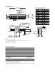
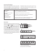
Display Internal Block Diagram
Figure 1 shows the internal block diagram of the HDSP-
253X display. The CMOS IC consists of an 8 byte Character
RAM, an 8 bit Flash RAM, a 128 character ASCII decoder, a
16 character UDC RAM, a UDC Address Register, a Control
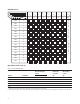
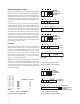
Figure 2. Logic levels to access the character RAM.
Character Ram
Figure 2 shows the logic levels needed to access the HDSP-
253X Character RAM. During a normal access the CE = “0”
and either RD = “0” or WR = “0”. However, erroneous data
may be written into the Character RAM if the Address lines
are unstable when CE = “0” regardless of the logic levels of
the RD or WR lines. Address lines A
0
-A
2
are used to select
the location in the Character RAM. Two types of data can
be stored in each Character RAM location: an ASCII code
or a UDC RAM address. Data bit D
7
is used to dierenti-
ate between the ASCII character and a UDC RAM address.
D
7
= 0 enables the ASCII decoder and D
7
= 1 enables the
UDC RAM. D
0
-D
6
are used to input ASCII data and D
0
-D
3
are used to input a UDC address.
CE
FL A
4
A
3
A
2
A
1
A
0
RST WR RD
CHARACTER
ADDRESS
SYMBOL IS ACCESSED IN LOCATION
SPECIFIED BY THE CHARACTER ADDRESS ABOVE
01
0 0
0 1
1
1 11
0
1 1
UNDEFINED
CONTROL SIGNALS
CHARACTER RAM ADDRESS
CHARACTER RAM DATA FORMAT
WRITE TO DISPLAY
READ FROM DISPLAY
UNDEFINED
000 = LEFT MOST
111 = RIGHT MOST
D
7
D
6
D
5
D
4
D
3
D
2
D
1
D
0
0 128 ASCII CODE
X X X UDC CODE1
DISPLAY
0 = LOGIC 0; 1 = LOGIC 1; X = DO NOT CARE
DIG
0
DIG
1
DIG
2
DIG
3
DIG
4
DIG
5
DIG
6
DIG
7
001 010 011 100 101 110 111000