
Datasheet


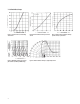
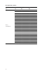


Figure 17. Recommended wave soldering prole
For product information and a complete list of distributors, please go to our web site: www.avagotech.com
Avago, Avago Technologies, and the A logo are trademarks of Avago Technologies in the United States and other countries.
Data subject to change. Copyright © 2005-2013 Avago Technologies. All rights reserved. Obsoletes 5989-4252EN
AV02-1555EN - August 22, 2013
LAMINAR WAVE
BOTTOM SIDE
OF PC BOARD
HOT AIR KNIFE
TURBULENT WAVE
FLUXING
PREHEAT
0 10 20
30
50
100
150
200
250
30 40 50
TIME – SECONDS
TEMPERATURE – C
60 70 80 90 100
TOP SIDE OF
PC BOARD
CONVEYOR SPEED = 1.83 M/MIN (6 FT/MIN)
PREHEAT SETTING = 150C (100C PCB)
SOLDER WAVE TEMPERATURE = 245C
AIR KNIFE AIR TEMPERATURE = 390C
AIR KNIFE DISTANCE = 1.91 mm (0.25 IN.)
AIR KNIFE ANGLE = 40
SOLDER: SN63; FLUX: RMA
NOTE: ALLOW FOR BOARDS TO BE
SUFFICIENTLY COOLED BEFORE EXERTING
MECHANICAL FORCE.
Precautions
Lead Forming
• The leads of an LED lamp may be preformed or cut to
length before they are inserted and soldered into the
PC board.
• If forming a lead is required before it is soldered, then
take care to avoid any excessive mechanical stress
induced to the LED package. Otherwise, cut the LED
leads to length after soldering at room temperature.
The solder joint formed will absorb the mechanical
stress of the lead cutting from traveling to the LED chip
die attach and wirebond.
• It is recommended that tooling be made precisely and
the leads cut to length, rather than relying on your
hand.
Soldering Conditions
• Care must be taken during PCB assembly and soldering
process to prevent damage to LED component.
• The closest an LED is allowed to be soldered on board is
1.59 mm below the body (encapsulant epoxy) for those
parts without stando.
• Recommended soldering conditions:
Wave Soldering Manual Solder Dipping
Pre-heat Temperature
105 °C Max.
–
Pre-heat Time 30 sec Max. –
Peak Temperature
250 °C Max. 260 °C Max.
Dwell Time 3 sec Max. 5 sec Max.
• The wave soldering parameter must be set and
maintained according to the recommended
temperature and dwell time in the solder wave.
Customer is advised to periodically check the soldering
prole to ensure the soldering prole used always
conforms to recommended soldering condition.
• If necessary, use a xture during soldering process to
hold the LED component in the proper orientation
with respect to the PCB.
• Proper handling is a must to avoid excessive thermal
stresses to LED components when heated. Therefore,
the soldered PCB must be allowed to cool to room
temperature, 25 °C, before handling.
• To ensure solderability, pay special attention to board
fabrication, solder masking, surface plating and lead
hole size and component orientation.
• Here are the recommended PC board plated through-
hole sizes for LED component leads:
LED Component
Lead Size
Diagonal Plated Through-
Hole Diameter
Lead size (typ.) 0.45 × 0.45 mm
(0.018 × 0.018 in.)
0.636 mm
(0.025 in)
0.98 to 1.08 mm
(0.039 to 0.043 in)
Dambar shear-
o area (max.)
0.65 mm
(0.026 in)
0.919 mm
(0.036 in)
Lead size (typ.) 0.50 × 0.50 mm
(0.020 × 0.020 in.)
0.707 mm
(0.028 in)
1.05 to 1.15 mm
(0.041 to 0.045 in)
Dambar shear-
o area (max.)
0.70 mm
(0.028 in)
0.99 mm
(0.039 in)
Note: Refer to application note AN1027 for more information on
soldering LED components.