
Datasheet

STM32F103xx Electrical characteristics
53/84
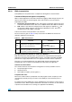
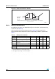
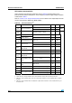
5.3.12 I/O port characteristics
General input/output characteristics
Unless otherwise specified, the parameters given in Ta bl e 33 are derived from tests
performed under the conditions summarized in Ta bl e 7. All I/Os are CMOS and TTL
compliant.
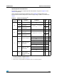
Table 33. I/O static characteristics
Symbol Parameter Conditions Min Typ
Max Unit
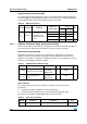
V
IL
Input low level voltage
(1)
1. Values based on characterization results, and not tested in production.
TTL ports
–0.5 0.8
V
V
IH
Standard IO input high level
voltage
(1)
2V
DD
+0.5
IO FT
(2)
input high level
voltage
(1)
2. FT = Five-volt tolerant.
25.5V
V
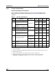
IL
Input low level voltage
(1)
CMOS ports
–0.5 0.35 V
DD
V
V
IH
Input high level voltage
(1)
0.65 V
DD
V
DD
+0.5
V
hys
Standard IO Schmitt trigger
voltage hysteresis
(3)
3. Hysteresis voltage between Schmitt trigger switching levels. Based on characterization results, not tested.
200 mV
IO FT Schmitt trigger voltage
hysteresis
(3)
5% V
DD
(4)
4. With a minimum of 100 mV.
mV
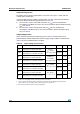
I
lkg
Input leakage current
(5)
5. Leakage could be higher than max. if negative current is injected on adjacent pins.
V
SS
≤V
IN
≤V
DD
Standard I/Os
±1
µA
V
IN
= 5 V
I/O FT
3
R
PU
Weak pull-up equivalent
resistor
(6)
6. Pull-up and pull-down resistors are designed with a true resistance in series with a switchable
PMOS/NMOS. This MOS/NMOS contribution to the series resistance is minimum (~10% order).
V
IN
= V
SS
30 40 50 kΩ
R
PD
Weak pull-down equivalent
resistor
(6)
V
IN
= V
DD
30 40 50 kΩ
C
IO
I/O pin capacitance 5 pF