
Datasheet

STM32F103xx Electrical characteristics
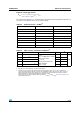
61/84
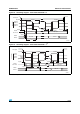
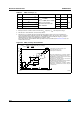
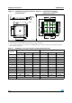
Figure 25. SPI timing diagram - slave mode and CPHA = 0
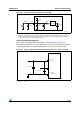
Figure 26. SPI timing diagram - slave mode and CPHA = 1
(1)
1. Measurement points are done at CMOS levels: 0.3V
DD
and 0.7V
DD
.
ai14134
SCK Input
CPHA= 0
MOSI
INPUT
MISO
OUT P UT
CPHA= 0
MS B O UT
MSB IN
BI T6 O U T
LSB IN
LSB OUT
CPOL=0
CPOL=1
BIT1 IN
NSS input
t
SU(NSS)
t
c(SCK)
t
h(NSS)
t
a(SO)
t
w(SCKH)
t
w(SCKL)
t
v(SO)
t
h(SO)
t
r(SCK)
t
f(SCK)
t
dis(SO)
t
su(SI)
t
h(SI)
ai14135
SCK Input
CPHA=1
MOSI
INPUT
MISO
OUT P UT
CPHA=1
MS B O UT
MSB IN
BI T6 O U T
LSB IN
LSB OUT
CPOL=0
CPOL=1
BIT1 IN
t
SU(NSS)
t
c(SCK)
t
h(NSS)
t
a(SO)
t
w(SCKH)
t
w(SCKL)
t
v(SO)
t
h(SO)
t
r(SCK)
t
f(SCK)
t
dis(SO)
t
su(SI)
t
h(SI)
NSS input