
Datasheet

Package characteristics STM32F103xx
70/84
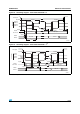
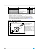
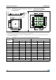
1. Drawing is not to scale.
2. The back-side pad is not internally connected to the V
SS
or V
DD
power pads.
3. There is an exposed die pad on the underside of the VFQFPN package. It should be soldered to the PCB. All leads should
also be soldered to the PCB.
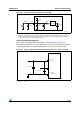
Figure 33. VFQFPN36 6 x 6 mm, 0.5 mm pitch,
package outline
(1)
Figure 34. Recommended footprint
(dimensions in mm)
(1)(2)(3)
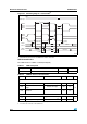
Seating plane
ddd C
C
A3
A1
AA2
D
e
28
36
Pin # 1 ID
R = 0.20
27
1
E
9
L
1018
D2
19
b
E2
ZR_ME
0.75
0.30
6.30
0.50
1.00
4.30
4.30
4.80
4.80 4.10
4.10
4.30
36
1
27
10
9
18
19
ai14870
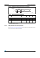
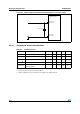
Table 49. VFQFPN36 6 x 6 mm, 0.5 mm pitch, package mechanical data
Symbol
millimeters inches
(1)
Min Typ Max Min Typ Max
A 0.800 0.900 1.000 0.0315 0.0354 0.0394
A1 0.020 0.050 0.0008 0.0020
A2 0.650 1.000 0.0256 0.0394
A3 0.250 0.0098
b 0.180 0.230 0.300 0.0071 0.0091 0.0118
D 5.875 6.000 6.125 0.2313 0.2362 0.2411
D2 1.750 3.700 4.250 0.0689 0.1457 0.1673
E 5.875 6.000 6.125 0.2313 0.2362 0.2411
E2 1.750 3.700 4.250 0.0689 0.1457 0.1673
e 0.450 0.500 0.550 0.0177 0.0197 0.0217
L 0.350 0.550 0.750 0.0138 0.0217 0.0295
ddd 0.080 0.0031
1. Values in inches are converted from mm and rounded to 4 decimal digits.