
Instructions


5
8025I–AVR–02/09
ATmega48P/88P/168P/328P
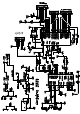
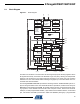
2.1 Block Diagram
Figure 2-1. Block Diagram
The AVR core combines a rich instruction set with 32 general purpose working registers. All the
32 registers are directly connected to the Arithmetic Logic Unit (ALU), allowing two independent
registers to be accessed in one single instruction executed in one clock cycle. The resulting
architecture is more code efficient while achieving throughputs up to ten times faster than con-
ventional CISC microcontrollers.
The ATmega48P/88P/168P/328P provides the following features: 4K/8K/16K/32K bytes of In-
System Programmable Flash with Read-While-Write capabilities, 256/512/512/1K bytes
EEPROM, 512/1K/1K/2K bytes SRAM, 23 general purpose I/O lines, 32 general purpose work-
ing registers, three flexible Timer/Counters with compare modes, internal and external
interrupts, a serial programmable USART, a byte-oriented 2-wire Serial Interface, an SPI serial
port, a 6-channel 10-bit ADC (8 channels in TQFP and QFN/MLF packages), a programmable
PORT C (7)PORT B (8)PORT D (8)
USART 0
8bit T/C 2
16bit T/C 18bit T/C 0 A/D Conv.
Internal
Bandgap
Analog
Comp.
SPI TWI
SRAMFlash
EEPROM
Watchdog
Oscillator
Watchdog
Timer
Oscillator
Circuits /
Clock
Generation
Power
Supervision
POR / BOD &
RESET
VCC
GND
PROGRAM
LOGIC
debugWIRE
2
GND
AREF
AVCC
DATABUS
ADC[6..7]PC[0..6]PB[0..7]PD[0..7]
6
RESET
XTAL[1..2]
CPU