
Product Specs


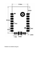


4
P15
I/O
P15 SD_CMD or SPI CSN or QSPI FLASH CSN
5
TX1
I/O
P11/UART1_TXD is usually used for debugging UART sending
6
RX1
I/O
P10/UART1_RXD is usually used for debugging UART receiving
7
P26/PWM5
I/O
P26 or IrDA input or PWM 5 or QSPI RAM CSN
8
P24/PWM4
I/O
P24 or low power clock output or PWM 4 or QSPI RAM clock
9
P23/ADC
I/O
P23 or ADC or JTAG TDO, or QSPI IO0 FLASH download data
output at download mode
10
REST
I
Chip enable, active high
11
P7/PWM1
I/O
P7 or Wi-Fi active output or PWM 1
12
P8/PWM2
I/O
P8 or Bluetooth active input or PWM 2
13
P9/PWM3
I/O
P9 or Bluetooth priority input or PWM 3
14
P17
I/O
P17 or SD Card DATA1 or SPI MISO or QSPI IO1
15
3V3
P
Power in dc 3.3V
16
GND
G
Power Ground
17
3V3
I
Power in dc 3.3V
18
TE
I
Chip enable, active high
19
P16
I/O
P16 or SD Card DATA0 or SPI MOSI or QSPI IO0
20
RX2
I/O
P1 port or UART2 RXD or I2C2 SDA, through
Commonly used for user UART receiving, rf calibration test
command control
21
TX2
I/O
P0 or UART2 TXD or I2C2 SCL, through
Commonly used for user UART transmission, rf calibration test
command control
22
P14
I/O
P14 or SD Card Clock or SPI Clock or QSPI FLASH clock
23
SI
I/O
P22 or Crystal clock output,or JTAG TDI or QSPI IO1
24
SO
I/O
P23 or ADC or JTAG TDO, or QSPI IO0 FLASH download data
output at download mode
九、Matters need attention:
A.As for the use environment of WIFI, wireless signals are easily affected by the surrounding
environment. For example, obstacles such as trees and metals will absorb wireless signals to
some extent, so that the distance of data transmission is affected to some extent in practical
applications.
B.It is recommended that the metal enclosure be not installed in the metal enclosure as it is
shielded from radio frequency signals.