
Instruction Manual

www.vishay.com For technical questions, contact: ind-modules@vishay.com
Document Number: 94427
2 Revision: 18-Jan-08
GA75TS120UPbF
Vishay High Power Products
"Half-Bridge" IGBT INT-A-PAK
(Ultrafast Speed IGBT), 75 A
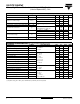
Note
(1)
Repetitive rating; V
GE
= 20 V, pulse width limited by maximum junction temperature
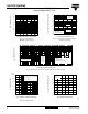
ELECTRICAL CHARACTERISTICS (T
J
= 25 °C unless otherwise specified)
PARAMETER SYMBOL TEST CONDITIONS MIN. TYP. MAX. UNITS
Collector to emitter breakdown voltage V
(BR)CES
V
GE
= 0 V, I
C
= 1 mA 1200 - -
VCollector to emitter voltage V
CE(on)
V
GE
= 15 V, I
C
= 75 A - 2.5 3.7
I
C
= 75 A, V
GE
= 15 V, T
J
= 125 °C - 2.25 3.3
Gate threshold voltage V
GE(th)
V
CE
= 6.0 V, I
C
= 750 µA
3.0 4.5 6.0
Temperature coefficient of threshold voltage ΔV
GE(th)
/ΔT
J
-- 14-mV/°C
Forward transconductance g
fe
V
CE
= 25 V, I
C
= 75 A
Pulse width 50 µs, single shot
- 107 - S
Collector to emitter leaking current I
CES
V
GE
= 0 V, V
CE
= 1200 V - 0.03 1.0
mA
V
GE
= 0 V, V
CE
= 1200 V, T
J
= 125 °C - 4.3 10
Diode forward voltage V
F
V
GE
= 0 V, I
F
= 75 A - 3 3.6
V
I
F
= 75 A, V
GE
= 0 V, T
J
= 125 °C - 2.83 3.3
Gate to emitter leakage current I
GES
V
GE
= ± 20 V - - 250 nA
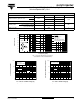
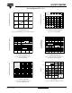
DYNAMIC CHARACTERISTICS (T
J
= 25 °C unless otherwise noted)
PARAMETER SYMBOL TEST CONDITIONS MIN. TYP. MAX. UNITS
Total gate charge (turn-on)
Q
g
V
CC
= 400 V
I
C
= 85 A
- 570 854
nC
Gate to emitter charge (turn-on)
Q
ge
- 96 144
Gate to collector charge (turn-on) Q
gc
- 189 283
Turn-on delay time
t
d(on)
R
G1
= 15 Ω
R
G2
= 0 Ω
I
C
= 75 A
V
CC
= 720 V
V
GE
= ± 15 V
Inductor load
T
J
= 125 °C
- 453 -
ns
Rise time t
r
-70-
Turn-off delay time t
d(off)
- 415 -
Fall time t
f
- 661 -
Turn-on switching energy
E
on
-8-
mJ
Turn-off switching energy
E
off
(1)
-11-
Total switching energy E
ts
(1)
-1932
Input capacitance C
ies
V
GE
= 0 V
V
CC
= 30 V
ƒ = 1 MHz
- 12 815 -
pFOutput capacitance C
oes
- 570 -
Reverse transfer capacitance C
res
- 110 -
Diode reverse recovery time t
rr
R
G1
= 15 Ω
R
G2
= 0 Ω
I
C
= 75 A
V
CC
= 720 V
dI/dt = 1300 A/µs
- 174 - ns
Diode peak reverse current I
rr
- 107 - A
Diode recovery charge Q
rr
- 9367 - nC
Diode peak rate of fall of recovery during t
b
dI
(rec)M
/dt - 1491 - A/µs