
User Manual


GB75YF120UT
www.vishay.com
Vishay Semiconductors
Revision: 21-Mar-13
2
Document Number: 93172
For technical questions within your region: DiodesAmericas@vishay.com
, DiodesAsia@vishay.com, DiodesEurope@vishay.com
THIS DOCUMENT IS SUBJECT TO CHANGE WITHOUT NOTICE. THE PRODUCTS DESCRIBED HEREIN AND THIS DOCUMENT
ARE SUBJECT TO SPECIFIC DISCLAIMERS, SET FORTH AT www.vishay.com/doc?91000
Note
(1)
Energy losses include “tail” and diode reverse recovery
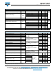
ELECTRICAL SPECIFICATIONS (T
J
= 25 °C unless otherwise specified)
PARAMETER SYMBOL TEST CONDITIONS MIN. TYP. MAX. UNITS
Collector to emitter breakdown voltage V
BR(CES)
V
GE
= 0 V, I
C
= 500 μA 1200 - -
VCollector to emitter voltage V
CE(ON)
I
C
= 75 A, V
GE
= 15 V - 3.4 4.0
I
C
= 100 A, V
GE
= 15 V - 3.8 4.5
I
C
= 75 A, V
GE
= 15 V, T
J
= 125 °C - 4.0 4.5
I
C
= 100 A, V
GE
= 15 V, T
J
= 125 °C - 4.53 5.1
Gate threshold voltage V
GE(th)
V
CE
= V
GE
, I
C
= 250 μA 4.0 5.0 6.0
Threshold voltage temperature coefficient V
GE(th)
/T
J
V
CE
= V
GE
, I
C
= 1 mA (25 °C to 125 °C) - - 11 - mV/°C
Zero gate voltage collector current I
CES
V
GE
= 0 V, V
CE
= 1200 V - 7 250
μA
V
GE
= 0 V, V
CE
= 1200 V, T
J
= 125 °C - 580 2000
Diode forward voltage drop V
FM
I
F
= 75 A - 3.7 4.9
V
I
F
= 100 A - 4.1 5.5
I
F
= 75 A, T
J
= 125 °C - 3.7 5.1
I
F
= 100 A, T
J
= 125 °C - 4.2 5.7
Gate to emitter leakage current I
GES
V
GE
= ± 20 V - - ± 200 nA
SWITCHING CHARACTERISTICS (T
J
= 25 °C unless otherwise noted)
PARAMETER SYMBOL TEST CONDITIONS MIN. TYP. MAX. UNITS
Total gate charge (turn-on) Q
G
I
C
= 75 A
V
CC
= 600 V
V
GE
= 15 V
- 630 -
nCGate to emitter charge (turn-on) Q
GE
-65-
Gate to collector charge (turn-on) Q
GC
- 250 -
Turn-on switching loss E
on
I
C
= 75 A, V
CC
= 600 V
V
GE
= 15 V, R
g
= 5 , L = 500 μH
T
J
= 25 °C
(1)
-1.74-
mJ
Turn-off switching loss E
off
-1.46-
Total switching loss E
tot
-3.20-
Turn-on switching loss E
on
I
C
= 75 A, V
CC
= 600 V
V
GE
= 15 V, R
g
= 5 , L = 500 μH
T
J
= 125 °C
(1)
-2.44-
Turn-off switching loss E
off
-2.35-
Total switching loss E
tot
-4.79-
Turn-on delay time t
d(on)
I
C
= 75 A, V
CC
= 600 V
V
GE
= 15 V, R
g
= 5 , L = 500 μH
T
J
= 125 °C
- 268 -
ns
Rise time t
r
-43-
Turn-off delay time t
d(off)
- 308 -
Fall time t
f
- 127 -
Reverse bias safe operating area RBSOA
T
J
= 150 °C, I
C
= 200 A
R
g
= 10 , V
GE
= 15 V to 0 V
Fullsquare
Short circuit safe operating area SCSOA
T
J
= 150 °C
V
CC
= 900 V, V
P
= 1200 V
R
g
= 10 , V
GE
= 15 V to 0 V
10 - - μs
Diode peak reverse recovery current I
rr
T
J
= 25 °C
V
CC
= 200 V
I
F
= 50 A
dI/dt = 10 A/μs
-1318
A
T
J
= 125 °C - 19 23
Diode reverse recovery time t
rr
T
J
= 25 °C - 132 189
ns
T
J
= 125 °C - 200 270
Total reverse recovery charge Q
rr
T
J
= 25 °C - 858 1700
nC
T
J
= 125 °C - 1900 3105