6121 Baker Road, Suite 108 Minnetonka, MN 55345 Phone (952) 933-6190 Fax (952) 933-6223 1-800-274-4284 www.chtechnology.com Thank you for downloading this document from C&H Technology, Inc. Please contact the C&H Technology team for the following questions - Technical Application Assembly Availability Pricing Phone – 1-800-274-4284 E-Mail – sales@chtechnology.com www.chtechnology.com - SPECIALISTS IN POWER ELECTRONIC COMPONENTS AND ASSEMBLIES - www.chtechnology.
VSKT320PbF Series www.vishay.com Vishay Semiconductors Thyristor/Thyristor (MAGN-A-PAK Power Modules), 320 A FEATURES • High voltage • Electrically isolated base plate • 3600 VRMS isolating voltage • Industrial standard package • Simplified mechanical designs, rapid assembly • High surge capability • Large creepage distances • UL approved file E78996 MAGN-A-PAK • Designed and qualified for industrial level • Material categorization: For definitions of compliance please see www.vishay.
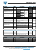
VSKT320PbF Series www.vishay.com Vishay Semiconductors ON-STATE CONDUCTION PARAMETER SYMBOL Maximum average on-state current at case temperature Maximum RMS on-state current Maximum peak, one-cycle on-state non-repetitive, surge current IT(AV) IT(RMS) ITSM TEST CONDITIONS 180° conduction, half sine wave 710 No voltage reapplied 100 % VRRM reapplied 7570 t = 10 ms No voltage reapplied t = 8.
VSKT320PbF Series www.vishay.com Vishay Semiconductors TRIGGERING PARAMETER SYMBOL TEST CONDITIONS VALUES PGM tp 5 ms, TJ = TJ maximum 10.0 Maximum average gate power PG(AV) f = 50 Hz, TJ = TJ maximum 2.0 Maximum peak gate current + IGM tp 5 ms, TJ = TJ maximum 3.0 Maximum peak negative gate voltage - VGT tp 5 ms, TJ = TJ maximum 5.0 Maximum peak gate power VGT Maximum required DC gate current to trigger IGT W A 4.
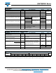
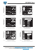
VSKT320PbF Series www.vishay.com Vishay Semiconductors Maximum Allowable Case Temperature (°C) RthJC(DC) = 0.125 K/W 120 110 Ø Conduction angle 100 90 30° 80 60° 90° 120° 70 180° Maximum Average On-State Power Loss (W) 130 60 0 50 100 150 200 250 300 350 Average On-State Current (A) 94085_01 650 600 550 500 450 400 350 300 250 200 150 100 50 0 200 300 400 500 Average On-State Current (A) Fig. 4 - On-State Power Loss Characteristics 8000 RthJC(DC) = 0.
VSKT320PbF Series Instantaneous On-State Current (A) www.vishay.com Vishay Semiconductors 10 000 TJ = 130 °C 1000 TJ = 25 °C Per junction 100 0.5 1.5 2.5 3.5 4.5 Instantaneous On-State Voltage (V) Fig. 7 - On-State Voltage Drop Characteristics 94085_07 ZthJC - Transient Thermal Impedance (°C/W) 1 Steady state value RthJC = 0.125 K/W (DC operation) 0.1 0.01 0.001 0.001 0.01 0.1 1 10 100 Square Wave Pulse Duration (s) Fig.
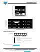
VSKT320PbF Series www.vishay.com Vishay Semiconductors CIRCUIT CONFIGURATION ~ ~ + + - K1 G1 G2 K2 LINKS TO RELATED DOCUMENTS Dimensions Revision: 05-Jul-12 www.vishay.com/doc?95086 Document Number: 94085 6 For technical questions within your region: DiodesAmericas@vishay.com, DiodesAsia@vishay.com, DiodesEurope@vishay.com THIS DOCUMENT IS SUBJECT TO CHANGE WITHOUT NOTICE. THE PRODUCTS DESCRIBED HEREIN AND THIS DOCUMENT ARE SUBJECT TO SPECIFIC DISCLAIMERS, SET FORTH AT www.vishay.
Legal Disclaimer Notice www.vishay.com Vishay Disclaimer ALL PRODUCT, PRODUCT SPECIFICATIONS AND DATA ARE SUBJECT TO CHANGE WITHOUT NOTICE TO IMPROVE RELIABILITY, FUNCTION OR DESIGN OR OTHERWISE. Vishay Intertechnology, Inc., its affiliates, agents, and employees, and all persons acting on its or their behalf (collectively, “Vishay”), disclaim any and all liability for any errors, inaccuracies or incompleteness contained in any datasheet or in any other disclosure relating to any product.