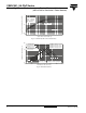
6121 Baker Road, Suite 108 Minnetonka, MN 55345 Phone (952) 933-6190 Fax (952) 933-6223 1-800-274-4284 www.chtechnology.com Thank you for downloading this document from C&H Technology, Inc. Please contact the C&H Technology team for the following questions - Technical Application Assembly Availability Pricing Phone – 1-800-274-4284 E-Mail – sales@chtechnology.com www.chtechnology.com - SPECIALISTS IN POWER ELECTRONIC COMPONENTS AND ASSEMBLIES - www.chtechnology.
VSKU/V41, 56..
VSKU/V41, 56..
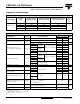
VSKU/V41, 56..PbF Series Thyristor/Thyristor, 45/60 A Vishay High Power Products TM (ADD-A-PAK Generation 5 Power Modules) TRIGGERING PARAMETER SYMBOL Maximum peak gate power Maximum average gate power Maximum peak gate current Maximum peak negative gate voltage Maximum gate voltage required to trigger TEST CONDITIONS PGM 10 PG(AV) 2.5 IGM 2.5 - VGM 10 VGT TJ = - 40 °C 4.0 TJ = 25 °C 2.
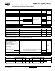
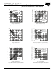
VSKU/V41, 56..PbF Series Thyristor/Thyristor, 45/60 A (ADD-A-PAKTM Generation 5 Power Modules) 130 VSK.41.. Series R thJC (DC) = 0.46 K/W 120 110 Conduction Angle 100 30° 60° 90° 120° 90 180° 80 0 10 20 30 40 50 Maximum Average On-state Power Loss (W) Maximum Allowable Case Temperature (°C) Vishay High Power Products 100 DC 180° 120° 90° 60° 30° 80 60 40 Conduction Period VSK.41..
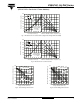
VSKU/V41, 56..PbF Series Thyristor/Thyristor, 45/60 A Vishay High Power Products TM (ADD-A-PAK Generation 5 Power Modules) SA R th 2 0. 300 K/ W 5K /W ta 0. el 200 3 -D 180° (Sine) 180° (Rect) W K/ .1 =0 0. 250 W K/ R Maximum Total Power Loss (W) 350 0. 7 150 K/ W 1K /W 100 2 x VSK.41.. Series Single Phase Bridge Connected T J = 125°C 50 1.5 K/ W 0 0 20 40 60 80 Total Output Current (A) 100 0 20 40 60 80 100 120 140 Maximum Allowable Ambient Temperature (°C) Fig.
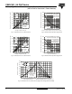
VSKU/V41, 56..PbF Series Thyristor/Thyristor, 45/60 A (ADD-A-PAKTM Generation 5 Power Modules) 90 Peak Half Sine Wave On-state Current (A) Maximum Average On-state Power Loss (W) Vishay High Power Products 180° 120° 90° 60° 30° 80 70 60 RMS Limit 50 40 30 Conduction Angle 20 VSK.56.. Series Per Junction TJ = 125°C 10 0 0 10 20 30 40 50 60 Peak Half Sine Wave On-state Current (A) Maximum Average On-state Power Loss (W) DC 180° 120° 90° 60° 30° RMS Limit Conduction Period 40 VSK.56..
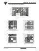
VSKU/V41, 56..PbF Series Thyristor/Thyristor, 45/60 A Vishay High Power Products TM (ADD-A-PAK Generation 5 Power Modules) Rt A hS 400 K/W 350 0. 3 K/ W -D Io W K/ 60° (Rect) 300 .1 =0 2 0. e lt 250 a 0.5 200 0.7 150 3 x VSK.56..
VSKU/V41, 56..PbF Series Vishay High Power Products Thyristor/Thyristor, 45/60 A (ADD-A-PAKTM Generation 5 Power Modules) Transient Thermal Impedance Z thJC (K/W) 1 Steady State Value: R thJC = 0.46 K/W R thJC = 0.40 K/W (DC Operation) VSK.41.. Series VSK.56.. Series 0.1 Per Junction 0.01 0.001 0.01 0.1 1 10 Square Wave Pulse Duration (s) Fig. 21 - Thermal Impedance ZthJC Characteristics Rectangular gate pulse a)Recommended load line for rated di/dt: 20 V, 30 ohms tr = 0.
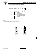
VSKU/V41, 56..PbF Series Thyristor/Thyristor, 45/60 A Vishay High Power Products TM (ADD-A-PAK Generation 5 Power Modules) ORDERING INFORMATION TABLE Device code VSK U 56 1 2 3 / 1 - Module type 2 - Circuit configuration: 16 P 4 5 U = Two SCR common cathode V = Two SCR common anode 3 - Current code 4 - Voltage code (see Voltage Ratings table) 5 - P = Lead (Pb)-free Note • To order the optional hardware go to www.vishay.com/doc?95172 CIRCUIT CONFIGURATION VSKU... VSKV...