
Specifications

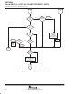


TNETX4090
ThunderSWITCH II
9-PORT 100-/1000-MBIT/S ETHERNET
SWITCH
SPWS044E – DECEMBER 1997 – REVISED AUGUST 1999
60
POST OFFICE BOX 655303 • DALLAS, TEXAS 75265
absolute maximum ratings over operating free-air temperature range (unless otherwise noted)
†
Supply voltage range, V
DD(2.5)
(see Note 1) –0.5 V to 2.7 V. . . . . . . . . . . . . . . . . . . . . . . . . . . . . . . . . . . . . . . . .
Supply voltage range, V
DD(3.3)
(see Note 1) –0.5 V to 3.6 V. . . . . . . . . . . . . . . . . . . . . . . . . . . . . . . . . . . . . . . . .
Supply voltage range, V
DD
a (see Note 1) –0.5 V to 2.7 V. . . . . . . . . . . . . . . . . . . . . . . . . . . . . . . . . . . . . . . . . . . .
Supply voltage range, DVREF (see Note 1) 1 V to 2.2 V. . . . . . . . . . . . . . . . . . . . . . . . . . . . . . . . . . . . . . . . . . . . .
Input voltage range, V
I
–0.5 V to V
DD(3.3)
+ 0.4 V. . . . . . . . . . . . . . . . . . . . . . . . . . . . . . . . . . . . . . . . . . . . . . . . . . .
Output voltage range, V
O
–0.5 V to V
DD(3.3)
+ 0.5 V. . . . . . . . . . . . . . . . . . . . . . . . . . . . . . . . . . . . . . . . . . . . . . . .
Input voltage range (RSL), V
IR
DVREF – 0.35 to DVREF + 0.8. . . . . . . . . . . . . . . . . . . . . . . . . . . . . . . . . . . . . .
Output voltage range (RSL), V
OR
0.0 to V
DD(2.5)
. . . . . . . . . . . . . . . . . . . . . . . . . . . . . . . . . . . . . . . . . . . . . . . . . . .
Thermal impedance, junction-to-ambient package, Z
θJA
: Airflow = 0 11.11°C/W. . . . . . . . . . . . . . . . . . . . . . . . .
Airflow = 100 ft/min 9.61°C/W. . . . . . . . . . . . . . . . .
Thermal impedance, junction-to-case package, Z
θJC
0.94°C/W. . . . . . . . . . . . . . . . . . . . . . . . . . . . . . . . . . . . . .
Operating case temperature range, T
C
0°C to 70°C. . . . . . . . . . . . . . . . . . . . . . . . . . . . . . . . . . . . . . . . . . . . . . . .
Storage temperature range, T
stg
–65°C to 150°C. . . . . . . . . . . . . . . . . . . . . . . . . . . . . . . . . . . . . . . . . . . . . . . . . . .
†
Stresses beyond those listed under “absolute maximum ratings” can cause permanent damage to the device. These are stress ratings only, and
functional operation of the device at these or any other conditions beyond those indicated under “recommended operating conditions” is not
implied. Exposure to absolute-maximum-rated conditions for extended periods can affect device reliability.
NOTE 1: All voltage values are with respect to GND.
recommended operating conditions
MIN NOM MAX UNIT
V
DD(2.5)
Supply voltage 2.5 2.6 2.7 V
V
DD(3.3)
Supply voltage 3 3.3 3.6 V
DVREF RSL reference voltage 1.8 2.0 2.2 V
V
I
Input voltage 0 V
DD(3.3)
V
V
O
Output voltage 0 V
DD(3.3)
V
V
IH
High-level input voltage 2 V
DD(3.3)
V
V
IL
Low-level input voltage (see Note 2) 0 0.8 V
I
OH
High-level output current –2 mA
I
OL
Low-level output current (except LED_DATA) 2 mA
I
OL
LED_DATA (terminal AE19) 0 8 mA
V
IHR
High-level input voltage (RSL) DVREF+0.35 DVREF+0.8 V
V
ILR
Low-level input voltage (RSL) (see Note 2) DVREF–0.35 DVREF–0.8 V
I
OHR
High-level output current (RSL) –10 10 µA
I
OLR
Low-level output current (RSL) 0 80 mA
NOTE 2: The algebraic convention, in which the more-negative (less-positive) limit is designated as a minimum, is used for logic-voltage levels
only.