
Owner's manual

Industrial Grade 203 Series PC Card Product Manual v3.0Cactus Technologies
®
28
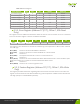
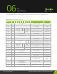
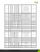
Data Register CE2- CE1- A0 Oset Data Bus
Word Data Register 0 0 X 0,8,9 D15-D0
Even Data Register 1 0 0 0,8 D7-D0
Odd Data Register 1 0 1 9 D7-D0
Odd Data Register 0 1 X 8,9 D15-D8
Error/Feature Register 1 0 1 1, Dh D7-D0
Error/Feature Register 0 1 X 1 D15-D8
Error/Feature Register 0 0 X Dh D15-D8
Table 5-25. Data Register
5.5.2. Error Register (Address-1F1[171]; Oset 1, 0Dh Read
Only)
This register contains additional information about the source of an error when an error is indicated
in bit 0 of the Status register. The bits are dened as follows:
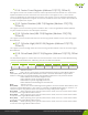
D7 D6 D5 D4 D3 D2 D1 D0
BBK UNC 0 IDNF 0 ABRT 0 AMNF
This register is also accessed on data bits D15-D8 during a write operation to oset 0 with -CE2 low
and -CE1 high.
Bit 7 (BBK) This bit is set when a Bad Block is detected.
Bit 6 (UNC) This bit is set when an Uncorrectable Error is encountered.
Bit 5 This bit is 0.
Bit 4 (IDNF) The requested sector ID is in error or cannot be found.
Bit 3 This bit is 0.
Bit 2 (Abort) This bit is set if the command has been aborted because of a status condition: (Not
Ready, Write Fault, etc.) or when an invalid command has been issued.
Bit 1 This bit is 0.
Bit 0 (AMNF) This bit is set in case of a general error.
5.5.3. Feature Register (Address-1F1[171]; Oset 1, 0Dh Write
Only)
This register provides information regarding features of the PC Card that the host can utilize. This
register is also accessed on data bits D15-D8 during a write operation to Oset 0 with CE2 low and
-CE1 high (except in True IDE Mode operation).