
Specifications

Si3220/25 Si3200/02
20 Preliminary Rev. 1.3
This product has
b
e
e
n
d
i
sc
o
n
t
inued.
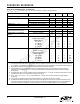
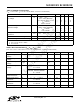
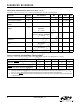
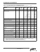
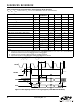
Table 14. Switching Characteristics—GCI Highway Serial Interface
(V
DD
, V
DD1
– V
DD4
= 3.13 to 5.25 V, T
A
= 0 to 70 °C for K/F-Grade, –40 to 85 °C for B/G-Grade)
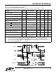
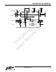
Figure 3. GCI Highway Interface Timing Diagram (2.048 MHz PCLK Mode)
Parameter
1
Symbol
Test
Conditions
Min Typ Max Units
PCLK Period (2.048 MHz PCLK Mode) t
p
—488—ns
PCLK Period (4.096 MHz PCLK Mode) t
p
—244—ns
FSYNC Period
2
t
fs
—125—µs
PCLK Duty Cycle Tolerance t
dty
40 50 60 %
FSYNC Jitter Tolerance t
jitter
——±120ns
Rise Time, PCLK t
r
——25ns
Fall Time, PCLK t
f
——25ns
Delay Time, PCLK Rise to DTX Active t
d1
——20ns
Delay Time, PCLK Rise to DTX Transition t
d2
——20ns
Delay Time, PCLK Rise to DTX Tristate
3
t
d3
——20ns
Setup Time, FSYNC
Rise to PCLK Fall t
su1
25 — — ns
Hold Time, PCLK Fall to FSYNC Fall t
h1
20 — — ns
Setup Time, DRX Transition to PCLK Fall t
su2
25 — — ns
Hold Time, PCLK Falling to DRX Transition t
h2
20 — — ns
FSYNC Pulse Width t
wfs
t
p
/2 — — ns
Notes:
1. All timing is referenced to the 50% level of the waveform. Input test levels are V
IH
= V
O
– 0.4 V, V
IL
= 0.4 V, rise and
fall times are referenced to the 20% and 80% levels of the waveform.
2. FSYNC source is assumed to be 8 kHz under all operating conditions.
3. Specification applies to PCLK fall to DTX tristate when that mode is selected.
t
su1
t
h1
t
p
t
r
t
f
t
h2
t
d3
t
d2
t
d1
PCLK
FSYNC
DRX
DTX
t
fs
t
su
2
Frame 0,
Bit 0
Frame 0,
Bit 0