
Specifications
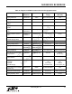
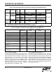

Si3220/25 Si3200/02
60 Preliminary Rev. 1.3
This product has
b
e
e
n
d
i
sc
o
n
t
inued.
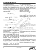
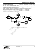
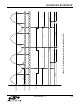
Figure 31. Si3225 External Ring Trip Circuitry
3.16.1. Ringing Relay Activation During Zero
Crossings
The Si3225 is for applications that use a centralized
ringing generator and a per-channel ringing relay to
connect the ringing signal to the TIP/RING pair. The
Si3225 has one relay driver output per channel (RRDa
and RRDb) that can drive a mechanical or solid-state
DPDT relay. To reduce impulse noise that can couple
into adjacent lines, the relay should be closed when
there is zero voltage across the relay contacts and
opened during periods when there is zero current
through the contacts.
3.16.2. Closing the Relay at Zero Voltage
Internal voltage monitoring circuitry closes the relay at
zero voltage with respect to the line voltage. By
observing the phase of the ringing signal and constantly
monitoring the open-circuit T-R voltage, V
OC
, the
Si3225 can detect the next time when there is zero
voltage across the relay contacts.
3.16.3. Opening the Relay at Zero Current
Opening the ringing relay at zero current also is
accomplished using the internal monitoring circuitry and
prevents arcing from excess current flow when the relay
contacts are opened. The current flowing through the
ringing relay is continuously monitored in the IRNGNG
RAM address, and two internal counters (COUNTER0
and COUNTER1) detect time elapsed since the last two
zero current crossings based on the ringing period and
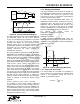
predict when the next zero crossing occurs. The ringing
relay current and internal counters are both updated at
an 8 kHz rate. To account for the mechanical delay of
the relay, a programmable advance firing timer allows
the user to initiate relay opening up to 10 ms prior to the
zero current crossing event. Figure 30 illustrates the
timing sequence for a typical ringing relay control
application.
During a typical ringing sequence, the Si3225 monitors
both the ringing relay current (IRNGNG) and the
RINGEN bit of the RINGCON register. The RINGEN bit
toggles because of pre-programmed ringing cadence or
a change in operating state. COUNTER0 and
COUNTER1 are restarted at each alternating zero
current crossing event, and the delay period,
ZERDELAY, equal to the ringing frequency period less
the desired advance firing time, D, is entered by the
user. If either counter reaches the same value as
ZERDELAY, the relay control signal is enabled when the
RINGEN bit transition has already occurred. During
typical ringing bursts, the LFS bits of the linefeed
register toggle between the RINGING and OHT states
based on the pre-programmed ringing cadence. The
transition from OHT to RINGING is synchronized with
the RRD state transitions, so the ringing burst starts
immediately. The transition from RINGING to OHT is
gated by a user-programmed delay period, LFSDELAY,
which ensures the ringing burst has ceased before
going to the OHT state or to the ACTIVE state in
response to a linefeed state change.
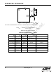
3.17. Polarity Reversal
The Dual ProSLIC devices support polarity reversal for
message-waiting functionality and various signaling
modes. The ramp rate can be programmed for a smooth
transition or an abrupt transition to accommodate
different application requirements. A wink function is
provided for special equipment that responds to a
smooth ramp to V
OC
= 0 V. Table 33 illustrates the
register bits required to program the polarity reversal
modes.
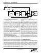
V
RING
V
OFF
806 k
806 k
510
+
_
Si3200
RING
TIP
Protection
Si3225
BLkRING
RTRP
Relay
Hook
Switch
Phone
VDD
RRD