
Specifications


Si3220/25 Si3200/02
70 Preliminary Rev. 1.3
This product has
b
e
e
n
d
i
sc
o
n
t
inued.
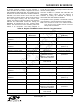
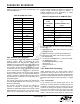
Table 40 outlines the hex codes corresponding to the
detected DTMF digits.
3.24. Modem Tone Detection
The Dual ProSLIC devices are capable of detecting a
2100 Hz modem tone as described in ITU-T
Recommendation V.8. The detection scheme can be
implemented in both transmit and receive paths and is
enabled by programming the appropriate register bit.
The detection scheme should be disabled for power
conservation after the modem tone window has passed.
Once a valid modem tone is detected, a register bit is
set accordingly, and the user can check the results by
reading the register value. A programmable debounce
interval is provided to eliminate false detection and can
be programmed in increments of 67 ms by writing to the
appropriate register.
The outputs of the 2100 Hz modem tone detectors are
located at RAM addresses 410 and 413 for the TX and
RX paths, respectively.
The contents of registers 410 and 413 indicate the
presence or absence of 2100 Hz energy. Table 41
indicates the relationship between the contents of these
RAM addresses and the level of the 2100 Hz energy
present in the corresponding signal path (TX or RX).
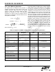
The threshold for declaring the presence or absence of
2100 Hz energy should be based on Table 41. A
suitable threshold for most applications is >0x20,
corresponding to a level of –15 dBm.
The following steps are used to access RAM address
410 and 413:
1. Write 0x02, 0x06, 0x0C, 0x00 to Reg. 87 (un-protect
test registers/bits)
2. Write 0x40 to Reg. 4 (access upper RAM space)
3. Write 0x02, 0x06, 0x0C, 0x00 to Reg. 87 (protect
test registers/bits)
4. For TX path use RAMAddress = 154 for the RX path
use RAMAddress = 157:
if (readRAM(RAMAddress) > 0x20)
Tone2100 Hz = 1;
else Tone2100 Hz = 0;
endif
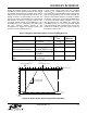
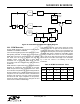
3.25. Audio Path Processing
Unlike traditional SLICs, the Dual ProSLIC devices
integrate the codec function into the same IC. The on-
chip 16-bit codec offers programmable gain/attenuation
blocks and multiple loopback modes for self testing. The
signal path block diagram is shown in Figure 11 on page
25.
3.25.1. Transmit Path
In the transmit path, the analog signal fed by the
external ac coupling capacitors is passed through an
anti-aliasing filter before being processed by the A/D
converter. An analog mute function is provided directly
prior to the A/D converter input. The output of the A/D
converter is an 8 kHz, 16-bit wide, linear PCM data
stream. The standard requirements for transmit path
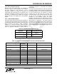
Table 40. DTMF Hex Codes
Digit Hex code
10x1
20x2
30x3
40x4
50x5
60x6
70x7
80x8
90x9
00xA
*0xB
#0xC
A0xD
B0xE
C0xF
D0x0
Table 41. 2100 Hz Level vs. RAM Hex Value
TIP and RING
Level
Across 600 W
(dBm)
TX Path: RAM 410 (154)
or
RX Path: RAM 413 (157)
(Hex)
+3 0x838
00x420
–3 0x20a
–6 0x107
–9 0x83
–12 0x41
–15 0x20