User Manual Brand Name:CALEX TECH Model Name: DongleBLE5
Any changes or modifications not expressly approved by the party responsible for compliance could void your authority to operate the equipment. Note: This equipment has been tested and found to comply with the limits for a Class B digital device, pursuant to part 15 of the FCC Rules. These limits are designed to provide reasonable protection against harmful interference in a residential installation.
1 Introduction The Bluetooth USB Dongle (PCA10059) is the preferred hardware to be used with the nRF Connect for Desktopsoftware package to develop and test your nRF-based wireless solutions. The hardware supports all theshort range wireless standards available on the nRF52 family of devices, and the built-in USB devicecontroller provides a high data throughput communication interface. The Bluetooth USB Dongle can also be used together with the nRF5 SDK for product development based on thenRF52840 SoC.
2 Minimum requirements Before you start, check that you have the required hardware and software.
Programmable Peripheral Interface - PPI High speed SPI interface 32MHz Quad SPI interface 32MHz EasyDMA for all digital interfaces RAM mapped FIFO using EasyDMA 12bit/200K SPS ADC 128 bit AES/ECB/CCM/AAR co-processor Single-ended antenna output (on-chip balun) On-chip DC-DC buck converter Quadrature demodulator Regulated supply for external components up to 25mA APPLICATIONS IoT - Smart Home products - Industrial mesh networks - Smart city infrastructure Advanced wearables - Connected watches - Advanced per
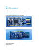
3 Kit content The nRF52840 Dongle consists of hardware (PCA10059), access to application firmware examples,documentation, hardware schematics, and layout files. 3.1 Hardware content The nRF52840 Dongle hardware consists of the board (PCA10059).
3.2 Downloadable content The nRF52840 Dongle downloadable content consists of a software tool, application firmware examples,and hardware files. Software •nRF Connect for Desktop Firmware package In the nRF5 SDK, you can find precompiled application firmware examples. Hardware files Schematics, layout, bill of materials, and Gerber files for nRF52840 Dongle (PCA10059) are included in azip file: • nRF52840 Dongle Hardware Files 3.
4 Getting started Complete a few steps to set up the hardware and install the required software. Before you start, check Minimum requirements on page 4. Connect the Dongle to a computer and get started with nRF Connect for Desktop. 1. Download and install nRF Connect for Desktop. This includes the driver for the nRF52840 USB Device Firmware Upgrade (DFU) feature. Fordocumentation on the tool, see nRF Connect. 2. Insert the nRF52840 Dongle in a USB port on your computer.
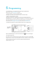
5 Programming The nRF52840 Dongle can be programmed through the built-in USB bootloader. Before you start, check Getting started on page 8. To program the Dongle, it must be in bootloader mode. The Dongle can be made to enter bootloader mode in one of the two ways: • Trigger the nRF52840 USB DFU endpoint. The firmware to support this is embedded in all nRF Connect for Desktop apps for the nRF52840Dongle.
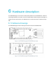
6 Hardware description The nRF52840 Dongle can be used as a development platform for the nRF52840 SoC. It features userconfigurable LEDs and a button as well as multiple GPIOs available along the board edges. In addition toradio communication, the nRF5240 SoC can communicate with a computer through USB. 6.1 Hardware drawings The nRF52840 Dongle hardware drawings show both sides of the PCA10059 board.
6.2 Block diagram The block diagram illustrates the nRF52840 Dongle functional architecture.
6.3 Power supply The nRF52840 Dongle can be powered from different sources. 6.3.1 Internal regulator The default power supply of the nRF52840 Dongle is the USB interface. The USB interface supplies powerto the on-chip high voltage regulator of the nRF52840 SoC. The output of the regulator supplies the SoC and the LEDs. The USB power connection (VBUS) is alsoavailable along the board edge. Next to VBUS, there is a connection point for VDD OUT, which is theoutput of the nRF52840 SoC high voltage regulator.
6.3.2 External regulated source The nRF52840 Dongle can also be configured to be supplied from an external regulated 1.8–3.6 V sourcethrough the VDD OUT connection point. To enable this, SB2 must be cut and SB1 must be soldered. 6.4 Buttons and LEDs The nRF528540 Dongle is equipped with a green LED (LD1), a multicolor RGB LED (LD2), a userconfigurable button (SW1), and a reset button (SW2). The LEDs and buttons are connected to dedicate I/Os on the nRF52840 SoC.
The buttons are active low, which means that the input will be connected to ground when the button isactivated. The SW1 button has no external pull-up resistor, but the reset button (SW2) has a 10 k pull-upresistor. To use SW1, P1.06 must be configured as an input with an internal pull-up resistor. The LEDs are active low, which means that writing a logical zero '0' to the output pin will illuminate theLED. 6.5 32.768 kHz crystal The nRF52840 Dongle is equipped with a 32.
6.6 USB The nRF52840 Dongle features a USB-A-type connector printed on the circuit board. Additional test points for the USB data lines are available on the bottom side of the circuit board if thenRF52840 Dongle is used as a module on a motherboard with a USB connector. To disconnect data linesfrom the onboard USB connector, cut solder bridges SB3 and SB4. Figure 9: Disconnecting USB data lines 6.7 SWD interface On the back side of the nRF52840 Dongle, there are connection points for the SWD interface.
6.8 External connections The nRF52840 Dongle has 15 GPIOs in addition to the ground, power, and SWD connections along thecastellated edges. The castellated edge holes have a pitch of 0.1 inches (2.54 mm) and a row spacing of 0.6 inches (15.24mm)2, making it suitable for stripboard connection. Test points for additional nine GPIOs are available onthe back side of the circuit board, leaving a total of 24 GPIOs accessible. Note: There is no reverse voltage protection on the power connections. 6.
Legal notices By using this documentation you agree to our terms and conditions of use. Nordic Semiconductor maychange these terms and conditions at any time without notice. Liability disclaimer Nordic Semiconductor ASA reserves the right to make changes without further notice to the product toimprove reliability, function, or design. Nordic Semiconductor ASA does not assume any liability arising outof the application or use of any product or circuits described herein.
Trademarks All trademarks, service marks, trade names, product names, and logos appearing in this documentationare the property of their respective owners. Copyright notice © 2018 Nordic Semiconductor ASA.All rights are reserved. Reproduction in whole or in part is prohibitedwithout the prior written permission of the copyright holder.