
User's Manual


MeshConnect™ Sub-G Module Series
Page 12
PROCESSING
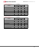
RecommendedReowProle
Parameters Values
Ramp up rate (from Tsoakmax to Tpeak) 3º/sec max
Minimum Soak Temperature 150ºC
Maximum Soak Temperature 200ºC
Soak Time 60-120 sec
TLiquidus 217ºC
Time above TL 60-150 sec
Tpeak 250ºC
Time within 5º of Tpeak 20-30 sec
Time from 25º to Tpeak 8 min max
Ramp down rate 6ºC/sec max
Pb-Free Solder Paste
Use of “No Clean” soldering paste is strongly recommended, as it does not require cleaning after the soldering process.
Note: The quality of solder joints on the castellations (‘half vias’) where they contact the host board should meet the appropriate IPC Speci-
cation. See the latest IPC-A-610 Acceptability of Electronic Assemblies, Castellated Terminations section.
Cleaning
In general, cleaning the populated modules is strongly discouraged. Residuals under the module cannot be easily removed
with any cleaning process.
• Cleaning with water can lead to capillary effects where water is absorbed into the gap between the host board and
the module. The combination of soldering ux residuals and encapsulated water could lead to short circuits between
neighboring pads. Water could also damage any stickers or labels.
• Cleaning with alcohol or a similar organic solvent will likely ood soldering ux residuals into the two housings, which
is not accessible for post-washing inspection. The solvent could also damage any stickers or labels.
• Ultrasonic cleaning could damage the module permanently.
The best approach is to consider using a “no clean” solder paste and eliminate the post-soldering cleaning step.
Optical Inspection
After soldering the Module to the host board, consider optical inspection to check the following:
• Proper alignment and centering of the module over the pads.
• Proper solder joints on all pads.
• Excessive solder or contacts to neighboring pads, or vias.
RepeatingReowSoldering
Only a single reow soldering process is encouraged for host boards.
Wave Soldering
If a wave soldering process is required on the host boards due to the presence of leaded components, only a single wave
soldering process is encouraged.