
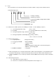
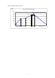
Specifications


− 6−
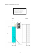
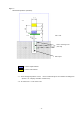
Figure -3
Antenna land-patterns (Tentative)
※ 1:Don't arrange the pattern on near, surface and inside layer to the antenna mounting area.
(Refer to our company evaluation circuit board.)
※ 2:A solder area is set at solder resist.
Land for input terminal
Land for NC terminal
50Ω input
Land for matching circuit
(1005 chip)
Unit:mm
※
2
※
1