
Operator`s manual
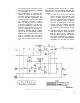
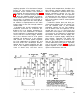
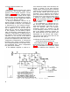
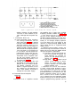
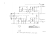

Figure 4. Receiver audio amplifier
lower Q2 have a common emitter resistor,
R6. Transistor Q2 operates near satura-
tion. Audio input signals from the audio
amplifier module are applied through iso-
lation resistor R2, attenuated by dropping
resistor R3, and are applied, through coup-
ling capacitor C2 to input amplifier Q1.
The audio output signals from Q1 are de-
veloped across collector load resistor R7
and directly coupled to the base of squelch
feedback amplifier Q3. The audio signals
amplified by transistor Q3 are developed
across a frequency selective (twin T) net-
work which acts as the collector load. Re-
sistors R10 and R11 and capacitor C 5 form
one T; capacitors C 3 and C4, and resistor
R12 form the other. This network is com-
parable to an antiresonant circuit; it ap-
plies minimum signal voltage to the base
of transistor Q2 at the frequency of 150
cps, and maximum signal voltage at other
frequencies. The signal applied to the base
of Q2 is degenerative to the signal at the
module A25, schematic diagram.
emitter of Q1. If the received audio signal
is modulated by a 150-cps tone, minimum
degenerative signal is applied to the base
of Q2. This action reduces the gain of Q1
at all frequencies except 150-cps. The bias
applied to the base of Q2 is determined
only by the voltage divider consisting of
resistors R9 and R13; transistor Q2 will
conduct and effectively cut off Q1 by virtue
of common emitter coupling across R6.
As a result, the bias applied to the base of
Q3 through the voltage divider, consisting
of resistors R8 and R7 and thermistor RT1,
is sufficient to cut off this stage.
b. When the 150-cps tone is present with
the incoming signal, the collector output of
feedback amplifier Q3, a 150-cps tone sig-
nal only, is filtered by the combination of
resistor R16 and capacitor C8 and is ap-
plied through coupling capacitor C7 to the
base of amplifier-detector Q4. With no sig-
nal input, the base of transistor Q4 is at
ground potential. Only the positive half
13