
Operator`s manual
(4)
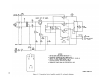
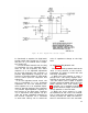
and A10J1 and current-limiting re-
sistor R7 to the anode of CM. This
positive voltage forward biases
CR2; the diode conducts heavily and
allows the regenerative circuit to
crystals Y13 and Y14 to be com-
pleted. If the RT-505/PRC-25 is
operating on a 100-kc channel (31.0
mc, 74.20 mc, etc), S1A will be in
the position shown and crystal Y13
(5.60 mc) will be selected through
contacts 8 and 11 of S1A to com-
plete the regenerative circuit to
the emitter of Q2.
If the RT-505/
PRC-25 is operating on a 50-kc
channel (31.15 mc, 74.25 mc, etc),
S1A will be turned clockwise one
position from that shown and crys-
tal Y14 (5.55 mc) will be selected
through contacts 8 and 9 of S1A to
complete the regenerative circuit
to the emitter of Q2.
Capacitor C7 is an rf bypass ca-
pacitor. Capacitor C8 is a coupling
capacitor between the base and
collector circuit. Resistors R10,
R11, and R12 develop fixed bias;
resistors R8 and R9 are emitter
swamping resistors for Q2.
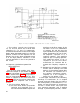
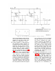
c. Buffer Q3.
(1)
(2)
The output from oscillator Q2 is
coupled through transformer T2
to the base and emitter of Q3. The
buffer isolates Q2 from any varying
loading effects.
Resistors R14, R15, and R16 de-
velop fixed-base bias. Resistor
R13 is the emitter swamping resis-
tor. Capacitors C11, C12, and C13
are rf bypass capacitors. Inductor
L2 and capacitor C15 form a de-
coupling network to prevent
rf leakage into the power supply.
The rf output from Q3 can be mess -
ured at test jack J3.
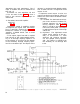
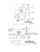
25. 53-Mc FiIter A13
(fig. 20)
The 53-mc filter has two input signals.
a. The output signal from 100-kc in-
terval oscillator module A
10 is coupled
through isolation resistor R1 and a match-
ing network consisting of capacitors C6
and C7 and transformer T3 to fss second
mixer module A12 (para 26). This circuit
minimizes spurious frequency injection
into the second mixer.
b. The 53-mc signal from first mixer
modu1e A14 is coupled to the filter
through transformer T1 to a triple-tuned
network. The three tuned circuits are the
secondary of T1 and C1, L1 and C3, T2
and C5. Capacitors C2 and C4 are coupl-
ling capacitors. This triple-tuned network
provides a 2-mc bandpass at the 3-
decibel (db) points. The output of this net-
work is coupled to second mixer module
A12.
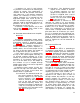
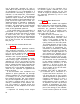
26. Frequency Synthesizer System Second
Mixer Module A12
(fig. 21)
The fss second mixer module heter-
odynes the output from 53-mc filter A13
(para 25), with the 46.85-mc to 47.75-mc
output of the 100-kc interval oscillator
(applied through A13) to produce an fss
if. of 5.55, 5.60, or 5.65 mc. This output
is applied to fss if. amplifier module A18
(para 27).
a. The 53-mc input from module A13
is coupled through capacitor C1 to the
base of Q1. The 46.85-mc to 47.75-mc in-
put from A13 is coupled through capacitor
C2 to the emitter of Q1. Transistor Q1
heterodynes these two input signals; the
resultant output signals at the collector of
Q1 are applied to the frequency selective
network.
b. The frequency selective network is
composed of capacitors C4 through C7,
variable transformers T1 and T2, and
variable inductors L1 and L2. The outputs
from Q1 are the two original frequencies
plus their sum and difference. The fre-
quency selective network passes only the
difference frequency. The network is a
bandpass filter having a flat characteristic
resonant frequency of 5.6 mc.
c. Resistor R5 and capacitor C 3 filter
rf signals from the +10-volt dc supply.
Resistors R1 and R2 provide the fixed-base
bias. Resistor R3 is the emitter swamping
resistor. Resistors R4 and R6 terminate
30