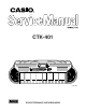
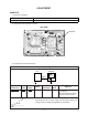
CTK-401 100 RHYTHMS 100 TONES TONE RHYTHM SONG BANK STATUS TEMPO VOLUME 100 SONG BANK (00-49) POWER/MODE 100 SONG BANK (50-99) MUSICAL INFORMATION SYSTEM MAIN SYNCHRO/ START/ VOLUME FILL-IN STOP TEMPO CHORD BOOK REW M m 7 M7 dim 3 4 TONE STOP FF SONG BANK FINGERED ON 0 CASIO CHORD OFF 1 5 6 aug sus4 NORMAL 2 7 8 LEFT ON/OFF RIGHT ON/OFF 9 PLAY/ ACCOMP VOLUME -5 add9 CLEAR RHYTHM TRANSPOSE/ TUNE SO NG PAUSE ER BANK CONTROLL 100 SONG BANK KEYBOARD MUSICAL INFORMATI
CONTENTS Specifications ................................................................................................................................... 1 Block Diagram .................................................................................................................................. 2 Circuit Description ............................................................................................................................ 3 Adjustment ................................................
SPECIFICATIONS GENERAL Keyboard: Tones: Polyphony: Auto accompaniment Rhythm patterns: Tempo: Chords: Rhythm controller: Accomp volume: Song bank Tunes: Controllers: Musical dictionary Name display: Tempo: Chord: Fingering: Song bank status: Staff: Keyboard: Other functions Transpose: Tuning: Volume: Terminals Phones/Output terminal: Power supply terminal: Power supply Batteries: Battery life: AC adaptor: Auto power off: Speaker output: Power consumption: Dimensions (HWD): Weight: 49 standard-size keys, 4
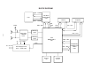
BLOCK DIAGRAM COM1 ~ COM16 LCD Driver SED1278F0A LSI3 LCD Buttons Keyboard SEG1 ~ SEG40 DB4 ~ DB7 Output —2— Power Amp.
CIRCUIT DESCRIPTION KEY MATRIX KI0 KI1 KI2 KI3 KI4 KI5 KI6 KO0 C2 G#2 E3 C4 G#4 E5 C6 KO1 C#2 A2 F3 C#4 A4 F5 KO2 D2 A#2 F#3 D4 A#4 F#5 KO3 D#2 B2 G3 D#4 B4 G5 KO4 E2 C3 G#3 E4 C5 G#5 KO5 F2 C#3 A3 F4 C#5 A5 KO6 F#2 D3 A#3 F#4 D5 A#5 KO7 G2 D#3 B3 G4 D#5 B5 KO8 — + 0 Tempo Down Tempo Up Volume Down Volume Up KO9 3 2 1 Accomp Volume 6 5 4 Synchro/ Fill-in Song Bank Chord Book KO10 Start/ Stop Transpose/ Tune Rhythm Tone KO1
CPU (LSI1: MSM6755B-17) The CPU reads sound data from the ROM in accordance with the pressed key and the selected tone; the CPU can read rhythm data simultaneously when a rhythm pattern is selected. Then it provides the left and the right channels’ waveforms separately, by converting the data into the waveforms with two built-in DACs. The CPU also controls key and button input. The following table shows the pin functions of LSI1. Pin No.
Pin No.
FILTER BLOCK Since the sound signals from the CPU is stepped waveforms, the filter block is added to smooth the waveforms. Amp. TA8248K CPU MSM6755B-17 Filter Block POWER AMPLIFIER (IC101: TA8248K) The power amplifier is a two-channel amplifier with standby switch. The following table shows the pin function of IC101. Pin No. Terminal In/Out Function 1 NC — Not used 2 B.S.2 — Terminal for a bootstrap capacitor 3 OUT2 Out 4 VCC In 5 OUT1 Out 6 B.S.
ADJUSTMENT MAIN PCB 1) Items to be adjusted: Item Measuring Instrument Vop voltage setting Voltmeter 2) Adjustment and Test Point Locations (TOP VIEW) Test point 3) Equipment connection/Procedure Vop voltage setting Set Voltmeter Output V5 Input Connection Input Point Input Signal Adjust VR1 Output Connection Output Point Voltmeter V5 Adjust for Adjust for 4.3 ±0.1 V reading on voltmeter. Make fine adjustment according to the next instruction. Eye Watching the LCD at a 53.
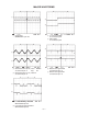
MAJOR WAVEFORMS 1 2 3 1 Clock pulse MSM6755B-17 pin 32 2 +5 V source DVDD JC connector pin 6 3 APO signal JC connector pin 5 6 4 7 5 6 Button scan signal KO6 JA connector pin 14 7 Button scan signal KO7 JA connector pin 15 4 Sound waveform (R-ch) Tone: Whistle JC connector pin 4 Key: A4 5 Sound waveform (L-ch) Volume: JC connector pin 3 8 9 8 LCD common signal COM9 SED1278F0A pin 55 9 LCD common signal COM10 SED1278F0A pin 56 —8—
PRINTED CIRCUIT BOARDS Main PCB JCM442-MA1M 1 5 4 3 6 2 7 Top View 8 Bottom View —9— 9
SCHEMATIC DIAGRAMS Main PCB JCM442-MA1M 2 3 4 5 6 1 9 8 — 11 — 7
Sub PCB JCM442-MA2M — 12 —
Keyboard PCBs KDM4910K-KY1M/KY2M — 13 —
COM7 COM6 COM5 COM4 COM3 COM2 COM1 SEG1 SEG2 SEG3 SEG4 SEG5 SEG6 SEG7 SEG8 SEG9 SEG10 SEG21 SEG22 SEG23 SEG24 SEG25 SEG26 SEG27 SEG28 SEG29 SEG30 SEG31 SEG32 SEG33 SEG34 SEG35 SEG36 SEG37 SEG38 SEG39 SEG40 COM7 COM6 COM5 COM4 COM3 COM2 COM1 SEG1 SEG2 SEG3 SEG4 SEG5 SEG6 SEG7 SEG8 SEG9 SEG10 SEG21 SEG22 SEG23 SEG24 SEG25 SEG26 SEG27 SEG28 SEG29 SEG30 SEG31 SEG32 SEG33 SEG34 SEG35 SEG36 SEG37 SEG38 SEG39 SEG40 Common COM11 COM12 SEG39 SEG40 COM10 COM9 COM14 COM15 COM16 SEG11 SEG12 SEG13 SEG14 SEG15 SEG16 S
EXPLODED VIEW 18 R-1 5 12 6 14 13 11 8 10 7 9 1 15 2 R-2 19 4 R-3 16 4 R-6 17 R-4 R-5 3 — 15 —
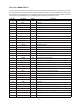
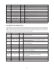
PARTS LIST CTK-401 Notes: This parts list does not include the cosmetic parts, which parts are marked with item No. "R-X" in the exploded view. Contact our spare parts department if you need these parts for refurbish. 1. Prices and specifications are subject to change without prior notice. 2. As for spare parts order and supply, refer to the "GUIDEBOOK for Spare parts Supply", published seperately. 3. The numbers in item column correspond to the same numbers in drawing.
Item Code No. Parts Name Main PCB 6926 0200 PCB/ASS'Y (MA1M) 2012 5603 LSI/MC (CPU) 2012 5611 LSI/MASK-ROM 2012 5569 LSI/LCD DRIVER 2012 1883 IC/MOS (RESET IC) 2252 1239 TRANSISTOR 2775 3286 POTENTIOMETER 2590 2100 OSCILLATOR/CERAMIC Sub PCB 2 6926 0190 PCB/ASS'Y (MA2, 3M) IC101 2114 5775 IC/LINEAR (POWER AMP.
MA0600571A