R (with price) CTK-100 CTK-100 ELECTRONIC KEYBOARD INDEX
CONTENTS SPECIFICATIONS .......................................................................................................... 1 BLOCK DIAGRAM ......................................................................................................... 2 CIRCUIT DESCRIPTION ................................................................................................ 3 TROUBLESHOOTING....................................................................................................
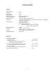
SPECIFICATIONS General Number of Keys: Polyphonic: Preset Tones: Auto-Rhythms: Auto-Accompaniment: Demonstration Tune: Built-In Speakers: Terminals: Power Source: Power Consumption: Dimentions: Weight: Standard Accessory: 49 8-note 100 100 CASIO Chord/Fingered Classical Medley 10 cm dia. 1.0W Input Rating: 2 pcs. Output Jack [Output Impedance: 120 Ω, Output Voltage: 3 V (rms)MAX], AC Adapter Jack (DC 9 V) 3-way AC or DC source AC: AC adapter AD-5 DC: 6 AA size dry batteries Battery life: Approx.
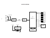
BLOCK DIAGRAM KO0~KO9 Output Jack CPU —2— MSM6387-13 Amplifier LA4598 Filter Main Volume KI0~KI7 T3/T4 Speakers Keyboard VC +9V VDD +5V Power supply circuit T2 Switches Oscillator
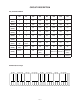
CIRCUIT DESCRIPTION Key and Switch Matrix KI0 KI1 KI2 KI3 KI4 KI5 KI6 KI7 KO0 (KC1) 0 1 C2 C#2 D2 D#2 E2 F2 KO1 (KC2) 2 3 F#2 G2 G#2 A2 A#2 B2 KO2 (KC3) 4 5 C3 C#3 D3 D#3 E3 F3 KO3 (KC4) 6 7 F#3 G3 G#3 A3 A#3 B3 KO4 (KC5) 8 9 C4 C#4 D4 D#4 E4 F4 KO5 (KC6) Tone Rhythm F#4 G4 G#4 A4 A#4 B4 KO6 (KC7) Tempo Up Tempo Down C5 C#5 D5 D#5 E5 F5 KO7 (KC8) Start/ Stop Fill-In F#5 G5 G#5 A5 A#5 B5 KO8 (KC9) Demo C6 Accomp.
CPU (MSM6387-13) The CPU contains a sound data ROM and a DAC (Digital to Analog Convertor), and it provides a sound waveform in accordance with the pressed key and the selected tone. The following table shows the pin functions of the CPU. Pin No. Terminal In/ Out Function 1, 2 TEST1, TEST2 3 RESET In Power ON reset terminal. When the power switch is turned on, the terminal receives a low level signal and the internal circuits of the LSI are initialized.
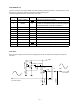
Power Amplifier (LA4598) The power amplifier is a 2-channel power amplifier with a standby switch. The following table shows the pin functions of the power amplifier. Pin No. Terminal In/Out Functiion 1 Power GND 2 Ch1 B.S. Out 3 Ch1 OUT In Channel1 output 4 VCC In +9 V source. Connected to the power source directly. 5 Ch1 N.F. In Negative feedback input 6 Ch1 IN In Channel1 input 7 D.C. 8 Pre GND In Ground (0 V) source 9 Standby In Power control signal input.
Power GND Ch1 B.S. Ch1 OUT VCC Ch1 N.F. Ch1 IN D.C. Pre GND Standby Ch2 IN Ch2 N.F. Ch2 OUT Ch2 B.S.
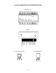
SCHEMATIC DIAGRAMS Keyboard PCBs M496K-KY1M, KY2M —7—
PCB VIEW and MAJOR WAVEFORMS 1 4 3 2 5 6 7 —8—
Main PCB M4502-MA1M 4.6 4 2.0 7 1.4 4.6 2.4 0.0 7.5 4.3 8.7 1.2 0.0 8.4 0.0 8.4 0.0 1.2 4.3 7.5 1 1.7 1 8.7 6.1 0.0 0.0 5.0 4.6 2.4 0.0 0.0 2.3 4.2 5.1 0.0 0.0 0.0 0.3 0.0 5.5 0.0 0.3 6 2 5 0.2 0.2 0.2 0.2 0.2 0.2 0.2 0.2 0.2 0.
EXPLODED VIEW — 10 —
PARTS LIST CTK-100 Notes: 1. Prices and specifications are subject to change without prior notice. 2. As for spare parts order and supply, refer to the "GUIDEBOOK for Spare parts Supply", published separately. 3. The numbers in item column correspond to the same numbers in drawing.
N N N N N Item Code No.
N Item JX JA N N N N N N N N N N N 1 2 3 4 5 6 7 8 9 10 11 11-1 11-2 11-3 12 13 14 15 16 17 18 19 20 21 22 23 Code No.
MA0300941A