(without price) QV-700 (KX-772) JAN.
CONTENTS SPECIFICATIONS ......................................................................................................................................1 WIRING AND BLOCK DIAGRAM ..............................................................................................................2 POWER SUPPLY CIRCUIT OPERATION .................................................................................................. 3 ADJUSTMENT ........................................................................
SPECIFICATIONS Item Specification Recording System Digital (JPEG base) Signal System NTSC Recording Medium Memory card (2 MB card included) Memory Capacity FINE; 14 images (Approx. 133 KB compressed) (2MB card) NORMAL; 26 images (Approx. 70 KB compressed) ECONOMY; 47 images (Approx.
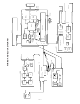
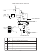
—2— Solenoid Photo INT Auto Iris Lens 5-pin Photo Sensor Comparator High Voltage Generator Strobe Ass'y IRISA/IRISB ADC CXD2310R Battery Voltage Battery Voltage Motor Driver CA-PCB CXD2452R CXD1267AN 3.3V CDS+AGC T.G 3.5V CB-PCB CXA2056Q Vdrv -5.5V 15V CCD Xenon Lamp 15V ICX098AK 3.5V 7-pin 23-pin GND Battery voltage Battery voltage GND 7-pin EEROM BR9040F 3.3V 20-pin FUNC button Detection Sw. (RSTW) L-PCB 60-pin 3.3V LED 3.
POWER SUPPLY CIRCUIT OPERATION VCC1-1 3 1 2 APO from Pin 202 of IC500 VCC1-1 Q580 2 IC586 5 VCC 1 2 IC584 FU152 R590 + 1 OUT NC 5 2 VDD 3 GND NC 4 VCC1-1 2 C525 4 GND 3 R585 IC582 1 1 2 Q582 3 7 6 Voltage detection signal 1 2 3 4 5 6 7 8 3 C592 1 PON from Key PCB Q588 VCC3-1 3 POB to Pin193 of IC500 8 CK VCC 7 PR D 6 CLR Q Q 5 GND 2 1 R593 R594 CN504 VCC3-1 PON KEY0 KEY1 KEY2 SHTTER GND GND IC588 C590 1 2 3 4 R592 VCC1-1 R595 VCC1-1 VCC1-1 R579 IC582 8 VCC 3 6 5 GND 4
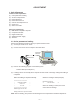
ADJUSTMENT 1. Unit Adjustment Contents of the adjustment (1) Color parameters loading (2) Scratch compensation (3) Flash adjustment (4) Flash function check (5) Current consumption check (6) Clock reset (7) Other test modes Necessary equipments (1) IBM PC/AT compatible computer (2) Computer link cable (3) Digital oscilloscope (4) Stabilized power supply (5) Ammeter 1-1. Color parameters loading Perform the following procedures when you replaced Camera Unit. (1) Set the QV-700 in “PLAY” mode.
1-2. Scratch compensation “Scratch” is a black dot which appears dimly on a white screen. Three scratches are allowable on 350,000 pxels screen. Perform this adjustment after loading color parameters. (1) Set the QV-700 in “REC” mode. (2) Set the dial on “ ”. (3) While pressing down the SHUTTER and DEL buttons, turn the power on. LCD screen indicates “TEST MODE”. (4) While TEST MODE is indicated on the LCD, select the dial on Press “MENU” and “ LCD indicates; . ” buttons simultaneously.
(1) Set the QV-700 in “REC” mode. (2) Execute the test program. • Set the dial on “ ”. • While holding down the “SHUTTER” and “DELETE” buttons, turn the POWER on. • While TEST MODE is indicated on the LCD, select the dial on Press “MENU” and “ LCD indicates; . ” buttons simultaneously. CLOCK RESET STROBE ADJUST DEFECT CORRECT BATTERY CHECK (4) Use “+” or “–” buttons to select “STROBE ADJUST” and press the SHUTTER button. (3) Shot a picture of the test paper.
(3) Set the QV-700 on “PLAY” mode and make sure that the picture taken is not too dark or too light. (4) After the shot, flash is charged automatically. Observing the ammeter, make sure that the charging current is less than 1.2 [A]. If the following pictures are taken, it may be caused by faulty wirings. Shrinken To solve this problem, install the wires as shown below. Red wire White wire 1-5.Current consumption (1) Set the QV-700 in “REC” mode.
(3) Using “+” or “–” buttons, select “CLOCK RESET” and press the SHUTTER button to execute the program. 1-7.Other test modes (1) Set the QV-700 in “REC” mode. (2) Execute the test program. • While holding down the “SHUTTER” and “DELETE” buttons, turn the POWER on. • While TEST MODE is indicated on the LCD, press “MENU” and “ LCD indicates; ” buttons simultaneously. BLACK COLOR BAR APO OFF (3) Using [ + ] or [ – ] buttons, select a test mode then press “SHUTTER”. 2.
2-1. VCC1, VCC3 voltage check Apply 5.0 ± 0.05 [V] on check point CP150. (For normal check you can use an AC adaptor however, when the camera is faulty, apply the above mentioned voltage.) (1) At Power on; VCC1 (CP164) ................. 3.2 ± 0.16 [V] VCC5-1 (CP165) .............. 5.25 ~4.75 [V] VCC5-2 (CP166) .............. 5.25~4.72 [V] VCC3-1 (CP167) .............. 3.3 ± 0.17 [V] VCC3-3 (CP168) .............. 3.3 ± 0.17 [V] VCC3-4 (CP169) .............. 3.3 ± 0.17 [V] (2) At Power off; VCC3-1 (CP164) ...
3.
3-1.VCC1 adjustment and VCC2, VCC6, VEE2, VCC0 voltage check Apply 5.0 ± 0.05 [V] on check point CP101. (For normal check you can use an AC adaptor however, when the camera is faulty, apply the above mentioned voltage.) (1) Adjust VR100 so that VCC1 is 4.50 ± 0.02 [V] (2) Check the following voltages. VCC2 ...................... 11.5 ~ 12.5 [V] VCC6 ...................... 17.5 ~ 19.5 [V] VEE2 ....................... -9.5 ~ -11.5 [V] VCC0 ...................... 2.8 ~ 3.
3-3.Backlight drive voltage adjustment Apply 5.0 ± 0.05 [V] on check point CP101. (For normal check you can use an AC adaptor however, when the camera is faulty, apply the above mentioned voltage.) (1) Adjust VR900 so that CP901 (VBL) is 11.5 ± 0.1 [V]. Also make sure that the current consumption is not abnormally large. 3-4.VCOM AC adjustment and VCOM DC coarse adjustment • Apply 5.0 ± 0.05 [V] on check point CP101.
3-5.Brightness voltage setting and contrast adjustment • Apply 5.0 ± 0.05 [V] on check point CP101. (For normal check you can use an AC adaptor however, when the camera is faulty, apply the above mentioned voltage.) • Input oscillation level 0.5 Vp-p standard video signal to VIDEO terminal (CP141) using a signal generator.(Normally you can use the signal from the digital PCB K772-DA however, when the camera is faulty, apply the above mentioned signal from signal generator.
3-6.Color adjustment • Perform this procedures together with TINT adjustment. • Perform this adjustment after contrast adjustment. • During the adjustment, make sure that the pedestal voltage of VB (CP324) signal is 5.0 ± 0.1 [V]. If not , perform the step (2) of “Brightness voltage setting and contrast adjustment”. • Apply 5.0 ± 0.05 [V] on check point CP101. (For normal check you can use an AC adaptor however, when the camera is faulty, apply the above mentioned voltage.) • Input oscillation level 0.
3-7.TINT adjustment • Perform this procedures together with COLOR adjustment. • Perform this adjustment after contrast adjustment. • During the adjustment, make sure that the pedestal voltage of VB (CP324) signal is 5.0 ± 0.1 [V]. If not , perform the step (2) of “Brightness voltage setting and contrast adjustment”. • Apply 5.0 ± 0.05 [V] on check point CP101. (For normal check you can use an AC adaptor however, when the camera is faulty, apply the above mentioned voltage.) • Input oscillation level 0.
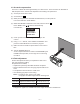
DISASSEMBLY The following explains the disassembly procedure of QV-700. Numbers in the procedures correspond to the part numbers on the exploded view. Assembly can be done by the reverse order. 1. Remove the CompactFlash card by pushing the release lever. 2. Remove two screws j from the bottom of the camera. 3. Unscrew two screws f from the lens side of the case. Note:Turn the lens as screws f are hidden by the Camera unit 1. 4.
5. Prying the case R, remove the battery cover and CompactFlash card cover. 6. Unhook the upper part of Case/Upper R and open the case. Unhook here 7. Desolder a lead wire from PCB Ass’y/Linear a and disconnect FPC from the connector CN514 on PCB Ass’y/Digital. Separate Case/Upper R and Case/Lower E. 8. Remove two screws g and disconnect two connectors from PCB A’ssy/Digital then separate Camera unit 1. 9. Remove two screws f from PCB Ass’y/Digital 2 and detach FPC from connector CN504.
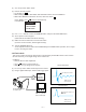
10.Lift up the buttom of the battery compartment and remove Holder/Battery 3 and PCB Ass’y/Digital. Note: Before you remove Holder/Battery 3, be sure that CompactFlash card release lever is in upright position. 11. Take Knob/Selector 6 and PCB Ass’y/Key 5 off the case. Note: Knob/Selector 6 can be removed by unscrewing two screws f from the bottom of the knob. 12.Peel Grip K then remove one screw h from Panel/Rear J. Unclip the E-ring from Pin J.
14.Lift up the stopper tab of connector CN700 and disconnect FPC cable. Also disconnect connector CN920. 15.Remove the BRIGHT knob T and take PCB Ass’y/Linear off the case. Note: Be careful not to bend or break the LED on the other side of the PCB. 16.Remove Three screws l from BL ass’y _ then remove the BL ass’y. Note: Do not touch BL ass’y with naked hand. 17.Remove Spacer ] and Display Ass’y [. Note: Do not touch Display Ass’y with naked hand. Camera Unit 18.Remove three screws h and m.
19.Peel off the caution label. Caution: Since high-voltage is applied on the circuits on Camera Unit, there is a risk of electric shock. Before proceeding to the following steps, discharge 70 µF, 300 V capacitor with a 1.5 kohm,5 W cement resistor. 1.5 kohm/5W resistor 20.Remove two screws and disconnect two wires red and white. 21.Remove Strobe unit 1-3 . 22.Remove two screws from the gear. Peel off the adhesive tape wrapped around the case shaft.
.Twisting the FPC cable and pulling out the connector throught the hole on the gear, pull the gear out. 24.Remove one screw l. 25.Disconnect FPC cables from the connectors CN200, CN201, and CN501 then remove CCD unit 1-2 .
PRINTED CIRCUIT BOARDS PCB K772-L Top view — 22 —
PCB K772-L Bottom view — 23 —
PCB K772-DA Top view — 24 —
PCB K772-DA Bottom view — 25 —
EXPLODED VIEW MAIN BODY 23 1 47 46 24 26 27 25 47 32 48 28 29 33 2 44 50 50 30 3 46 34 36 31 35 51 3-1 49 37 2-1 3-2 46 38 39 4 40 45 8 59 3-3 10 7 9 5 6 5-1 11 12 13 14 16 46 15 17 48 18 52 19 42 52 52 20 55 41 22 43 48 21 — 26 — 52 41-1
CAMERA UNIT 1-1 1-2 48 1-3 53 54 52 1-4 1-10 1-7 1-9 1-5 1-6 1-8 1-11 — 27 —
PARTS LIST LINEAR Item D110 D111 D112 D113 D700 D710 D900 IC100 IC130 IC300 IC350 IC700 IC701 IC900 IC920 D140 Q100 Q140 Q141 Q900 Q901 Q950 SW140 SW141 T100 T900 VR302 PCB ASS'Y Code No.
DIGITAL Item D151 D155 D160 D161 D170 D171 D510 D513 D525 D660 FU150 FU151 FU152 IC150 IC152 IC156 IC400 IC500 IC503 IC505 IC507 IC510 IC515 IC529 IC530 IC531 IC540 IC545 IC550 IC580 IC582 IC584 IC586 IC588 IC651 IC652 JK150 JK510 JK515 SW502 Q155 Q156 Q158 Q159 Q169 Q507 Q508 Q510 Q511 PCB ASS'Y Code No.
Item Code No.
MAIN BODY COMPONENT Item Code No.
Item Code No.
ACCESSORY Item Code No.
SCHEMATIC DIAGRAMS PCB L772-L Display Controller To Back Light To Digital PCB To LCD Chroma IC For Strobe — 34 —
+5 V Power Supply Circuit +3.2 V Video Signal Block Video Out AC Adapter Jack To Linear PCB Battery Voltage PCB K772-DA +3.3 V Power Supply Circuit YUV Processor Communicaiton Blcok +15.0 V RS-232C Jack –5.
KEY — 36 —
CASIO TECHNO CO.,LTD.