
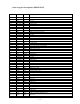
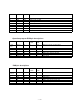
Specifications

— 9 —
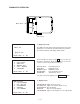
VIN
VSS
KAC
KIO
ADDRESS BUS
2 MHz
VDD1
ON
MAIN SWITCH
SW
GND
VDD
(Pin53)
(Pin54)
(Pin41)
VDD
"H"
"H"
ADDRESS
DATA
VDD
"L"
OSCO
OSCI
(Pin70)
INT0
V2ON
Gate array
DATA BUS
(Pin40)
(Pin45)
(Pin36)
"L"
(Pin24)
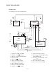
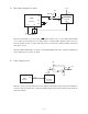
System chart
The circuitry operates in the following order:
1. Supply 5V to VDD1 and VDD2.
2. Output "L" from SWO terminal.
3. Output "L" from IC4 and Q5 terminal.
4. Main switch ON.
5. Input "L" to SW terminal.
6. Input "L" from KAC terminal.
7. Push power on button switch.
8. CPU oscillation is generated.
9. Output "H" from V2ON terminal.
10. Output "L" from VOB terminal.
OFF
CIRCUIT EXPLANATIONS
CPU
HD62076C03
PDN
"L"
SWO
"L"
2
3
5
4
6
7
µPD23C2001EGW-344
(Operation program)
ROM
VOB
OEO
(Pin62)
(Pin35)
"L"
12
(Pin58)
(Pin28)
MSO
(Pin49)
"L"
13
14
15
(Pin24)
(Pin22)
Power supply
circuit
V1~V5
for LCD
IC4
1
VDD
Low battery
detector
9
8
11. Output all LCD drive voltages.
12. Gate array sends ROM output enable
signal to OE terminal.
13. Gate array sends ROM Chip enable
signal to CE terminal.
14. CPU sends address to ROM.
15. CPU receives data from ROM.
SSC2571F0A
CE
OE
GND
11
10