
User's Manual


This document is exclusive property of CHIPSEA and shall not be reproduced or copied or transformed to any other format
without prior permission of CHIPSEA
6/11 NO:CS-QR-YF-054A02
Gathering ICs bit by bit and forming vast sea.
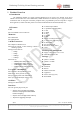
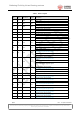
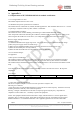
Table 1 Pin description
QFN48
No.
QFN32
No.
Pin name Type Description
1 1 P00 I/O
General purpose input/output0
JTAG_TDO
2 2 P01 I/O
General purpose input/output1
JTAG_TDI
3 3 P02 I/O
General purpose input/outpu2
JTAG_TMS
4 4 P03 I/O
General purpose input/output3
JTAG_TCK
9 5 BOOT0 I Boot_select[0]
20 13 P14 I/O
General purpose input/output14
AIO3
21 14 P15 I/O
General purpose input/output15
AIO4
25 18 P16 I/O
General purpose input/output16
AIO5
32K crystal input
26 19 P17 I/O
General purpose input/output17
AIO6
32K crystal output
27 20 P18 I/O
General purpose input/output18
*Note: Not support interrupt function
AIO7
PGA differential positive input
28 21 P19 I/O
General purpose input/output19
*Note: Not support interrupt function
AIO8
PGA differential negative input
29 22 P20 I/O
General purpose input/output20
*Note: Not support interrupt function
AIO9
Micphone bias output
30 23 RST_N I
reset pin, low level active
37 26 P23 I/O
General purpose input/output23
*Note: Not support interrupt function
38 27 P24 I/O
General purpose input/output24
*Note: Not support interrupt function
Boot_select[1]
39 28 P25 I/O
General purpose input/output25
*Note: Not support interrupt function
Boot_select[2]
45 29 P31 I/O
General purpose input/output31
*Note: Not support interrupt function
46 30 P32 I/O
General purpose input/output32
*Note: Not support interrupt function
47 31 P33 I/O
General purpose input/output33
*Note: Not support interrupt function
48 32 P34 I/O
General purpose input/output34
*Note: Not support interrupt function