
User's Manual


This document is exclusive property of CHIPSEA and shall not be reproduced or copied or transformed to any other format
without prior permission of CHIPSEA
7/11 NO:CS-QR-YF-054A02
Gathering ICs bit by bit and forming vast sea.
2 Electrical Specifications
2.1 Absolute Maximum Ratings
Maximum ratings are the extreme limits to which CSM92F30 Module can be exposed
without permanently damaging it. Exposure to absolute maximum ratings for prolonged
periods of time may affect the reliability of the CSM92F30 Module.Table2 Specifies the
absolute maximum ratings for CSM92F30 Module.
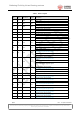
Table 13 CSM92F30 Module Absolute Maximum Ratings
Symbol Range Unit
Supply voltage 0~3.6 V
I/O pin voltage -0.3~VIN+0.3 V
Operating temperature -40~+125 ºC
Storage temperature -55~+150 ºC
Solder temperature,time 220ºC,10s
2.2 DC Characteristics
Table 14 DC Characteristics
Symbol Parameter Min. Typ. Max. Unit
VIN
Supply voltage, normal
mode
1.8 3.3 3.6 V
VIH Digital input high level VIN-0.3 - VIN+0.3 V
VIL Digital input low level 0 - 0.3 V
VOH Digital output high level VIN-0.3 - VIN+0.3 V
VOL Digital output low level 0 - 0.3 V
2.3 Receiver Specification
Table 15 Receiver Specification
Parameter Min. Typ. Max. Unit
Receive sensitivity@ 125Kbps GFSK -103 dBm
Receive sensitivity @500Kbps GFSK -98 dBm
Receive sensitivity @1Mbps BLE -97 dBm
Receive sensitivity@2Mbps BLE -94 dBm
Maximum input signal level -5 dBm