
Specifications

CINTERION
®
BGS12 Hardware Interface Description
Contents
31 of 109
Page
BGS12 HID_V00.915
Confidential / Released
2019
-
01
-
07
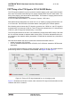
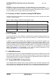
2) After reset: BGS12 has finished the reset action and has not entered the firmware initiali-
zation state.
3) Firmware initialization: The software has taken the control right of hardware, and begins to
initialize the firmware.
At reset state is reached with the rising edge of the EMERG_RST signal - either after a nor-
mal module startup (see Section 3.3.1.1) or after a reset (see Section 3.3.2.2). When BGS12
passes through at reset state and after reset state, the firmware initialization state begins.
The firmware initialization is completed as soon as the ASC0 interface lines CTS0, DSR0 and
RING0 as well as the ASC1 interface line CTS1 have turned high (see Section 3.7 and
Section 3.8). At that time, the module is ready to receive and transmit data.
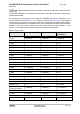
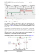
Table 7: Signal states
Signal name At reset After reset Firmware
initialization
CCIN I / 166K PD I / 166K PD I /166K PD
CCRST L L O / L
CCIO L L I O / L
CCCLK L L O / L
RXD0 I / 166K PD I / 166K PD O / H
TXD0 I / 166K PD I / 166K PD I
CTS0 I / 166K PD I / 166K PD O / H
RTS0 I / 166K PD I / 166K PD I / 166K PU
RING0 I / 166K PD I / 166K PD O / H
DTR0 I / 166K PD I / 166K PD I / 166K PU
DCD0 I / 166K PD I / 166K PD O / 166K PU
DSR0 I / 166K PD I / 166K PD O / 166K PU
RXD1 O / 166K PU O / 166K PU O / H
TXD1 I / 166K PU I / 166K PU I
RXD2 I / 166K PD I / 166K PD O / H
TXD2 I / 166K PD I / 166K PD I
CTS2 I / 33K PD I / 33K PD O / H
RTS2 I / 33K PD I / 33K PD I / 33K PU
FAST_SHTDWN I / 166K PD I / 166K PD I / 166K PU
GPIO5 / LED O / L O / L O / 33K PU
GPIO6 /
Jamming Indicator
I / 166K PD I / 166K PD I O / 166K PU
GPIO7 I / 166K PD I / 166K PD I O / 166K PU
GPIO8 I / 166K PD I / 166K PD I O / 166K PU
GPIO9 / I2CCLK O / L O / L O / 33K PU
GPIO10 / I2CDAT O / L O / L I O / 33K PU