
Specifications


CINTERION
®
BGS12 Hardware Interface Description
Contents
72 of 109
Page
BGS12 HID_V00.915
Confidential / Released
2019
-
01
-
07
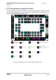
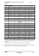
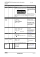
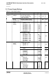
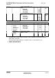
Table 20: Pad assignments
Pad no. Signal name Pad no. Signal name Pad no. Signal name
1
VMIC
27
GPIO10/I2CDAT
53
BATT
+RF
2
EPN
28
GPIO9/I2CCLK
54 GND
3
EPP
29
TXD1
55 GND
4
GND 30
RXD1
56 GND
5
BATT
+BB
31
Do not use
57 GND
6
GND
32
Do not use
58 GND
7
Do not use
33
EMERG_RST
59 RF_OUT
8
ON
34
GND
60 GND
9
GND
35
NC
61
GND
10
VDIG
36
GPIO8
62 GND
11
RXD0
37
GPIO7
63 GND
12
CTS0
38
GPIO6/
Jamming
Indicator
64 AGND
13
TXD0
39
GPIO5/LED
65 MICP
14
RING0
40
FAST_SHTDWN
66 MICN
15 RTS0 41 DSR0 67-97 GND
16
VDDLP
42
DCD0
98 Do not use
17
CCRST
43
DTR0
99-106 GND
18
CCIN
44
Do not use
245 GND
19
CCIO
45 Do not use 246 RTS2
20
CCVCC
46 Do not use 247 CTS2
21
CCCLK
47 GND 248 RXD2
22
NC
48 GND 249 TXD2
23
IISDO 49 GND
250 GND
24
IISLRCK
50 GND 251 GND
25
IISDI
51 GND 252 GND
26
IISCLK
52 GND
1. The pads 67-106 are centrally located and should be connected to Ground except for pad
98 that is not used. Pad 98 should not be connected to the external appli- cation, but should
be left open.
Signal pads that are not used should not be connected to an external application.
Please note that the reference voltages listed in Table 21 are the values measured directly on
the BGS12 module. They do not apply to the accessories connected.