
Specifications


CINTERION
®
BGS12 Hardware Interface Description
Contents
73 of 109
Page
BGS12 HID_V00.915
Confidential / Released
2019
-
01
-
07
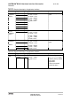
Table 21: Electrical description of application interface
Function Signal IO Signal form and level Comment
Power
supply
BATT
+BB
BATT
+RF
I
V
I
max = 4.35V V
I
norm
= 3.8V
V
I
min = 3.2V
1
during Tx burst on board
C
I
C=0 2.1A
C=2200uF
0.92A
C=4400uF 0.62A
Lines of BATT
+BB
or
BATT
+RF
and GND must be
connected in parallel for
supply purposes because
higher peak currents may
occur.
C is the capacitor connecting with VBAT
pins.
I is the peak current of Tx burst
at EGSM
network.
Minimum voltage must
not fall below 3.2V includ-
ing drop, ripple, spikes.
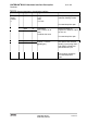
Power GND
Ground Application Ground
External
supply
voltage
VDIG
O
Normal operation: V
O
norm
= 2.80V ±3%
I
O
max = -50mA
SLEEP mode Operation:
V
O
Sleep = 2.80V ±5%
I
O
max = -50mA
VDIG may be used for
application circuits.
If unused keep line open.
Not available in Power
Down mode. The exter-
nal digital logic must not
cause any spikes or
glitches on VDIG.
Ignition ON
I
R
I
1M ±15%
V
IH
max = VDDLP + 0.5V
V
IH
min = 1.2V at ~12µA
V
IL
max = 0.2V
|¯ _¯ _¯ _¯ _ high impulse
This signal switches the
module ON.
This line must be driven
high by an open drain or
open collector driver
connected to VDDLP.
See Section 3.3.
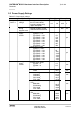
Emergency
shutdown
EMERG_
RST
I
V
I
H
max = V
BAT
V
I
H
min =1.2V
V
IL
max =0.2V
~~| |~~ low impulse width > 1ms
This line must be driven
low by an open drain or
open collector driver con-
nected to GND.
If unused keep line open.
Fast
shutdown
FAST_S
HTDWN
I
V
IL
max = 0.84V
V
IH
min = 1.96V
V
IH
max = 3.1V
This line must be driven
low.
If unused keep line
open.
~~| |~~ low impulse width = 10ms
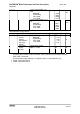
RTC
backup
VDDLP I/O
V
O
norm = 3.0V ±10%
I
O
max = 1.6mA
V
I
max = 3.3V
V
I
min = 2.6V
I
I
typ = 170µA
It is recommended to use
a serial resistor between
VDDLP and a possible
capacitor. See 3.3.1.1.
If unused keep line open.